NOTE: This article appeared in Issue 315 of Circuit Cellar, back in October 2016. I’ve posted it here for your reading pleasure as well. References to previous articles are for Circuit Cellar Issues, as this was originally written for the print publication. This version differs slightly from the print version – this is my own ‘author copy’ version before the Circuit Cellar editing.
Back in December 2015, I discussed how I solder BGA devices (such as FPGAs) using a low-cost reflow oven. This article will discuss the design of the FPGA board itself, which you could then assemble using the tips in my previous article.
I’ll assume you have a rough idea of what external parts you need, as they will be highly dependant on what you are trying to accomplish with your design. In addition to design-specific information, there are a few standards external requirements such as programming interface, communications, and power. This article will briefly cover some of these external requirements, but the concentration of this article is how to physically lay-out the FPGA board at a reasonable cost.
Some of the topics I covered previously too – for example in my June 2015 article I discussed the use of a generic USB microcontroller as a FPGA interface chip, which is very useful if you need to shuffle data to/from the FPGA.
So let’s assume you have a (mostly) complete schematic, and are wondering how to make this a reality. Let’s start with setting a target goal in terms of board requirements.
PCB Specifications
Assuming this design will be either a prototype run or possibly a small production run, it makes sense to design your PCB with specific requirements in mind to keep costs reasonable. The two PCB specifications you are most commonly told are the minimum “trace/space” (that is, minimum width of a trace, and minimum spacing between copper features), and the minimum drill size.
As I mentioned in my previous article, I’m often using an overseas PCB fab at 3pcb.com, although many other options are worth trying. They offer a variety of trace/space and drill size options, so I’ll target a 5 mil space/trace with 0.2 mm drill. This is a fairly “standard” technology option, so shouldn’t be a problem when moving towards a small production run (i.e., Qty 100-200).
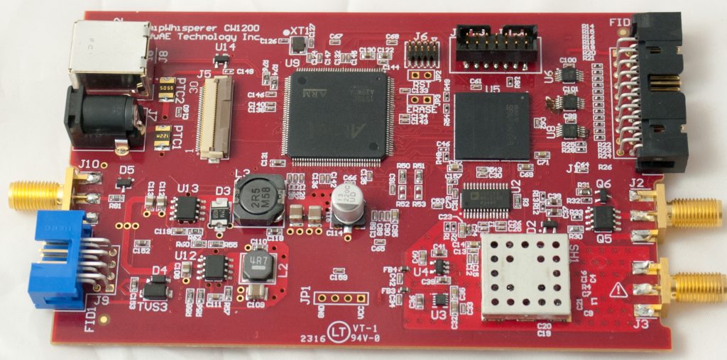
To give you an idea of what we’re working with, Figure 1 shows an example of the final PCB I designed and assembled. This uses a Spartan 6 LX45 FPGA with an Atmel SAM3U microcontroller for high-speed USB communications.
Layer Cake
In this example, I’m targeting a 6-layer PCB. While you can get away with a 4-layer in some circumstances, it often results in trade-offs that I’d rather avoid. If you were targeting a more advanced design with DDR memory, I’d consider a 6-layer board the absolute minimum, with an 8-layer PCB being a fairly likely option.
The stack-up of layers I’m using is given in Figure 2. This stack-up was the default for a local fab house (Lazer-Tech Ltd., in Ontario, Canada) that I’d be using when moving towards a production run. While I didn’t validate if the overseas fab actually respected this stack-up, there were no controlled impedances required so it was unlikely to affect my “alpha” prototype. I built a second validation unit based on the boards from the production run to confirm the actual stack-up had the required performance.

Using 6 layers allows me to have a solid unbroken ground plane, and a mostly unbroken power plane. The FPGA requires multiple voltages, so I’ve chosen to use a split power plane which is mostly a 3.3V plane, with a small island of 1.2V for the internal VCC voltage required by the FPGA. This power plane split requires very careful consideration to avoid routing signals across it.
Every signal needs somewhere for the return current to flow. Assuming this is a high-speed signal (such as clock, databus, etc.) we want the return current to flow as close underneath the signal as possible. Note this return current is a high-frequency signal, and for example may not need to actually flow on the ground plane. Instead it’s possible for the return current to flow elsewhere, and be coupled to the ground plane via a decoupling capacitor.
Layers 1 & 3 can use Layer 2 (the ground plane) as the reference, whereas Layers 4 & 6 can use Layer 5 (the VCC plane) as a reference. This means every signal layer has an plane layer next to it. The split in Layer 5 means that if you route a signal across the power plane split, the return current has to flow around this split, as in Figure 3. If you want to see a real-life example of what happens, see my blog post on the topic.

For high-speed signals, it’s important to avoiding switching the reference plane too. For example, if I was routing a signal on the top layer (Layer 1), then use a via to go to the bottom layer (Layer 6), this would mean the reference current will be transitioning from Layer 2 to 5 as well. While in an ideal world high-speed signals wouldn’t change layers at all, if you do change layers it’s best to for example go from Layer 1 to 3, so the return current is always flowing on Layer 2.
Decoupling capacitors connect the GND and VCC plane throughout the PCB (i.e., not only at ICs, but are sprinkled throughout too). This is done to provide a return path for any stray currents due to such layer switches.
You might notice from the stack-up that layers 3 & 4 are closer together than they are to their respective reference planes. This was a downside of using the default stack-up, as ideally I’d increase the space between layers 3 & 4 and have a reduced space between layer 3 to 2 and 4 to 5. One could also match the spacing between the layers and their reference planes, which would be helpful if you needed controlled impedances (I didn’t for this design).
There are a number of other issues regarding signal integrity (SI) to be aware of; I can’t hope to cover them here, but I can point you in the right direction. If you’re looking for an online course to guide you through this area, two I recommend are: Andy Eadie’s “EMC Pre-compliance” course at EMCFastPass.com which covers a number of issues related to both signal integrity and electro-magnetic compliance; and Dr. Eric Bogatin runs the SI Academy at www.bethesignal.com which dives into more advanced SI topics. A great recent example of a specific SI issue is in Robert Lacoste’s article “Digital Line Terminations” in the April 2016 issue of Circuit Cellar, as he has some demonstrations on real test boards.
As mentioned, one critical aspect of high-speed signals is to avoid routing the signal across a break in the plane. This might happen because you’ve cheated and done a bit of signal routing on a power layer (very likely in a more constrained 4-layer PCB), or you have split planes. Due to the nature of FPGA projects it may be required that a signal gets routed across a split plane, for example because the VCC-IO for an always-on microcontroller isn’t connected to the VCC-IO for the FPGA which is switched on and off.
This means the signal will be required to transition between two different reference planes. In this case it’s best to connect the split planes with decoupling capacitors, as in Figure 4. While not ideal, it provides a path for any return current flowing in the split plane to cross between. In Figure 4 the top-layer traces in red actually have an unbroken ground plane as a reference (not visible in the figure), so I’ve still tried to minimize the signals flowing over a split plane. Only the bottom-layer traces should use the split VCC layer as a reference plane.

Even if you go to the trouble of having an unbroken plane, you might accidently create trouble with dense vias. Everywhere you have a via means some clearance around internal planes that the vias do not connect to. Enough vias close together will result in an effective slot in that internal plane, as in Figure 5.

This can get really troublesome if you have a split plane supplying power to the FPGA, something common in practice due to the multiple voltages required. Underneath the FPGA also tends to have a dense concentration of vias due to the signal breakout required. In my board there’s a number of vias for both GND and VCC-IO (3.3V) surrounding the VCC-INT pins. These “other” vias will pierce the VCC-INT island, and cause a chunk of copper to be removed from the island.
A handy option in my design tool (Altium Designer) is something called the “PDN Analyzer”, which helps you understand what sort of voltage drops you might see on the power distribution network (PDN). As it can be almost impossible to avoid these holes in dense boards, the PDN analyzer provides a useful resource to simulate your voltage drop, and also visualize the current density to ensure you won’t cause problems in the physical PCB. Figure 6 shows an example of the PDN visualization, where there is about a 50 mV expected drop from a 3A current draw.

Using the PDN Analyzer, I was able to see some excessively high current density. This high current density was due to narrow slivers of power plane between vias that were piercing the VCC-INT island. Rearranging the vias solved the problem, and avoided potential issues such as local heating of those slivers of copper due to the high current density.
VIA Trouble
Piercing the power plane isn’t the only potential trouble you can have. You may also find that your FPGA package requires a more advanced (and thus expensive) PCB technology than you planned on using.
The BGA in this board is a CSG324 package from Xilinx, which has a finer 0.8mm pitch than the 1.0mm pitch FTG256 package I used in my December 2015 article. This causes a bit of a problem when we go to break-out the FPGA, which you can see in Figure 7. The spacing between break-out vias is too narrow to allow a 5-mil trace/space. This will create islands where we cannot break out certain balls, since we can’t route a trace between the vias.

But this assumes every layer has the same ring around the via drill hole. Thus the solution is to (carefully) use vias with incomplete stack-ups. That is to say they do not have a full copper ring on each layer. This is shown in Figure 8, where you can see for example certain vias have no connection to inner layer(s). Figure 8 shows how the trace in Figure 7 was successfully routed between the vias – the vias on either side of that trace have no copper ring on the associated layer.

Give me the Power
So far I’ve concentrated on the physical design of the board, and have skipped over the electrical design. I’ll briefly summarize some considerations around additional FPGA support resources required here.
The first thing you’ll need is a suitable power supply. The requirements here will vary drastically based on specifics of your design – for example if you had a design with external DDR3 memory, you’ll need to supply considerably more power for the IO drivers related to that bus compared to a simple SRAM interface.
Luckily, the FPGA vendors (such as Xilinx and Altera) provide tools to estimate the power consumption based on estimates of your design (such as number and standards of IOs, speeds of clocks, approximate resource utilization, etc.). This lets you design an appropriate power supply without over-engineering the design.
Most likely you’ll need a switch-mode power supply. Many different vendors provide highly reliable switch-mode power supply controllers, which by following the suggested circuit and layout can be used with great reliability. On this example board I’m using the Alpha & Omega Semiconductor AOZ1094 and AOZ1021 switch-mode buck regulators for the VCC-INT and VCC-IO supplies respectively, as had used them previously on a similar design so simply copied that onto this board.
Losing your Mind
One other standard consideration is the FPGA configuration memory. At minimum you should always route the JTAG header out, as it makes the most reliable “first contact” for checking the board design and FPGA is working correctly. For Xilinx FPGAs, I normally use the small 2mm header that plugs into the configuration cable, which is Molex part number 0878321420.
Lately, all of my FPGA designs are configured from a bitstream downloaded over USB (known as slave serial mode). Despite this I always design a SPI FLASH memory chip onto the board, such that the FPGA could be configured to operate from a power-on bitstream if needed.
You can even mount the majority of the parts if you want, as in Figure 9. Here by mounting resistor R46 I can enable the SPI flash output to drive the configuration DIN pin. SPI flash memory mounted like this can be configured through the JTAG programming tool, making it a very easy way for boards to power-on live.

Keep the Beat
The final standard across all designs will be clock input(s). Many designs simply use an external oscillator mounted somewhere that drives a FPGA global CLK pin. You may also be able to use a clock output from a microcontroller on your board, saving the cost of an additional oscillator.
These clock signals should always be routed to a global clock pin. If you’re using the newer 7-series Xilinx products, note that the GCLK pins come in positive/negative pairs, designed to accept differential clock inputs.
If using them single-ended you can only use the positive input – don’t try routing a clock to the negative side! So for example if on your schematic you have a pin called “IO_L13P_T2_MRCC_14” and “IO_L13N_T2_MRCC_14”, you can only route a clock to the first of those two inputs.
If you have complete control over the clock input pin, you should also check for any restrictions on the global clock pins. As mentioned in my June 2016 article, the “Global” in global clock input can be a little misleading. If it’s a very early prototype it doesn’t hurt to either break out extra clock pins, or even add spare oscillator pads that you don’t populate. If it turns out it’s better to input the clock to a different region, or if you need a different frequency, having the pads there makes it an easier job than trying to fly-wire something in later.
While this article has been just a quick overview, hopefully it gives you some confidence to design your own FPGA board using the latest devices. It’s possible to design and assemble a board at reasonable costs, showing it’s something that a small engineering company or even a well-equipped hobbyist is capable of doing.
RESOURCES
December 2015 Programmable Logic in Practice Article, Circuit Cellar Magazine
April 2016 The Darker Side Column, Circuit Cellar Magazine
June 2016 Programmable Logic in Practice Article, Circuit Cellar Magazine
EMC Fast-Pass EMC Pre-Compliance Course: www.emcfastpass.com
Teledyne Lecroy S.I. Academy: www.bethesignal.com
Blog post showing real-life split plane results: http://colinoflynn.com/2013/04/split-ground-plane-example-of-failing-high-speed-signals/