What’s inside of Apple’s new AirTag? There was already an iFixIt teardown (which I swear was missing a few items that are there now), but of course was curious to see what sort of protection was enabled. Notably the nRF chip used is likely vulnerable to a known bypass of security as well. With that in mind, I set out to see how we could dump some data from this thing – the good news is you can access a lot of interesting stuff (including the SPI flash) right from the backside, which requires you to simply pop the first plastic cover off. This is super-easy to do without damaging anything. Going further than that is tricky to keep it all intact.
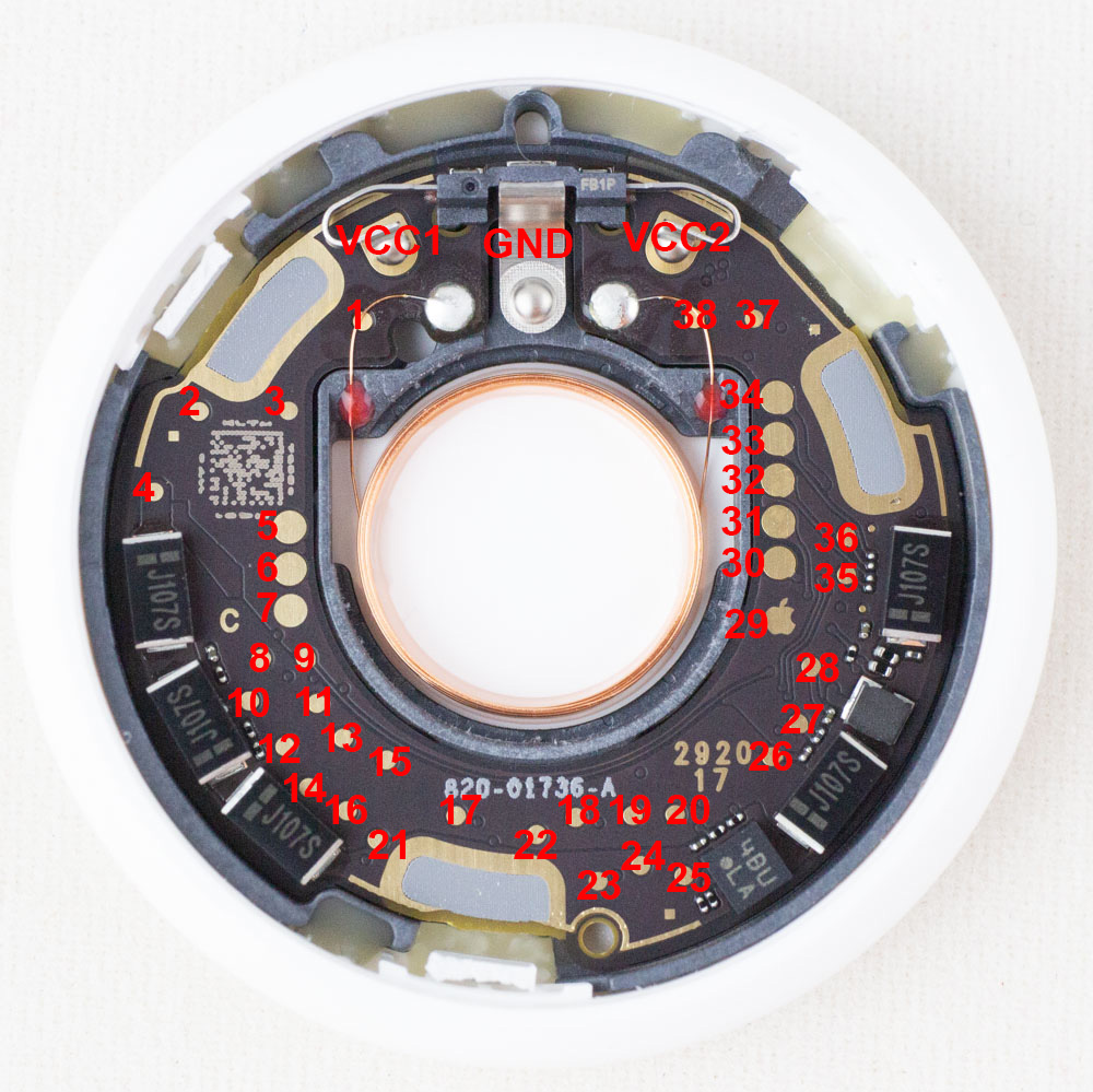
If you want to jump right to the answers, check out my AirTag-RE repo on github where I list the known test points that will be of interest. You can also see my twitter thread where I started the teardown:
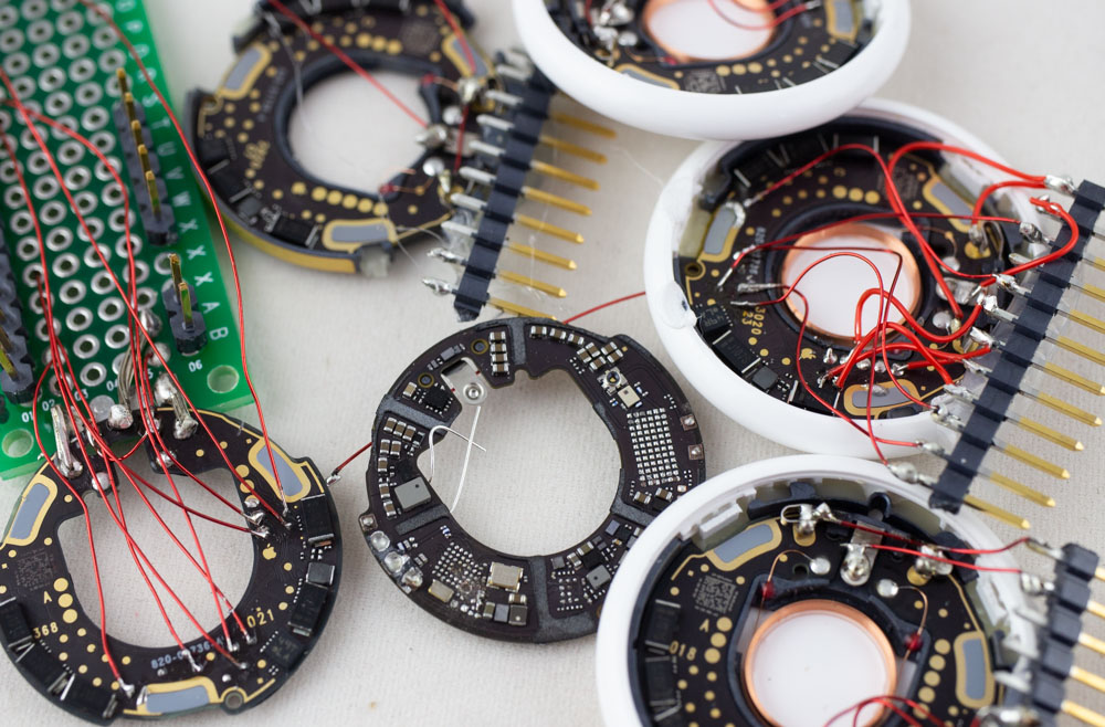
To remove the board from the AirTab, the best way is to bend the case to the side like this:
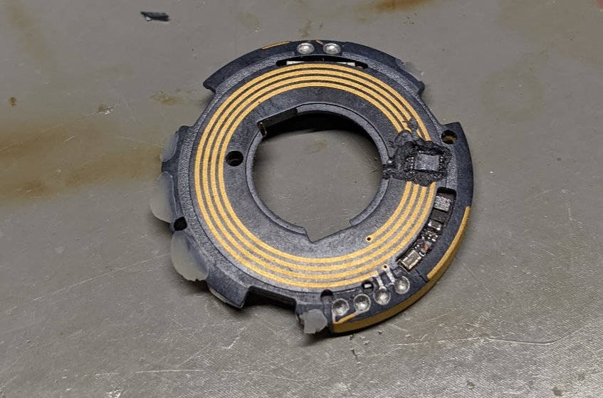
The center PCB with plastic enclosure just pops out. The plastic part includes the various antennas which are printed onto it – if you remove the PCB from the black plastic enclosure you will rip the antenna solder points. Once you do that, you’ll be rewarded with the back view of the PCB:
The solder joints at the edges are the antenna connections which ripped off (4x at upper center and 2x bottom left-of-center). The nRF chip has a NFC and Bluetooth antenna present. If you try to use the board like this, you need at minimum to add the bluetooth antenna back as shown here:
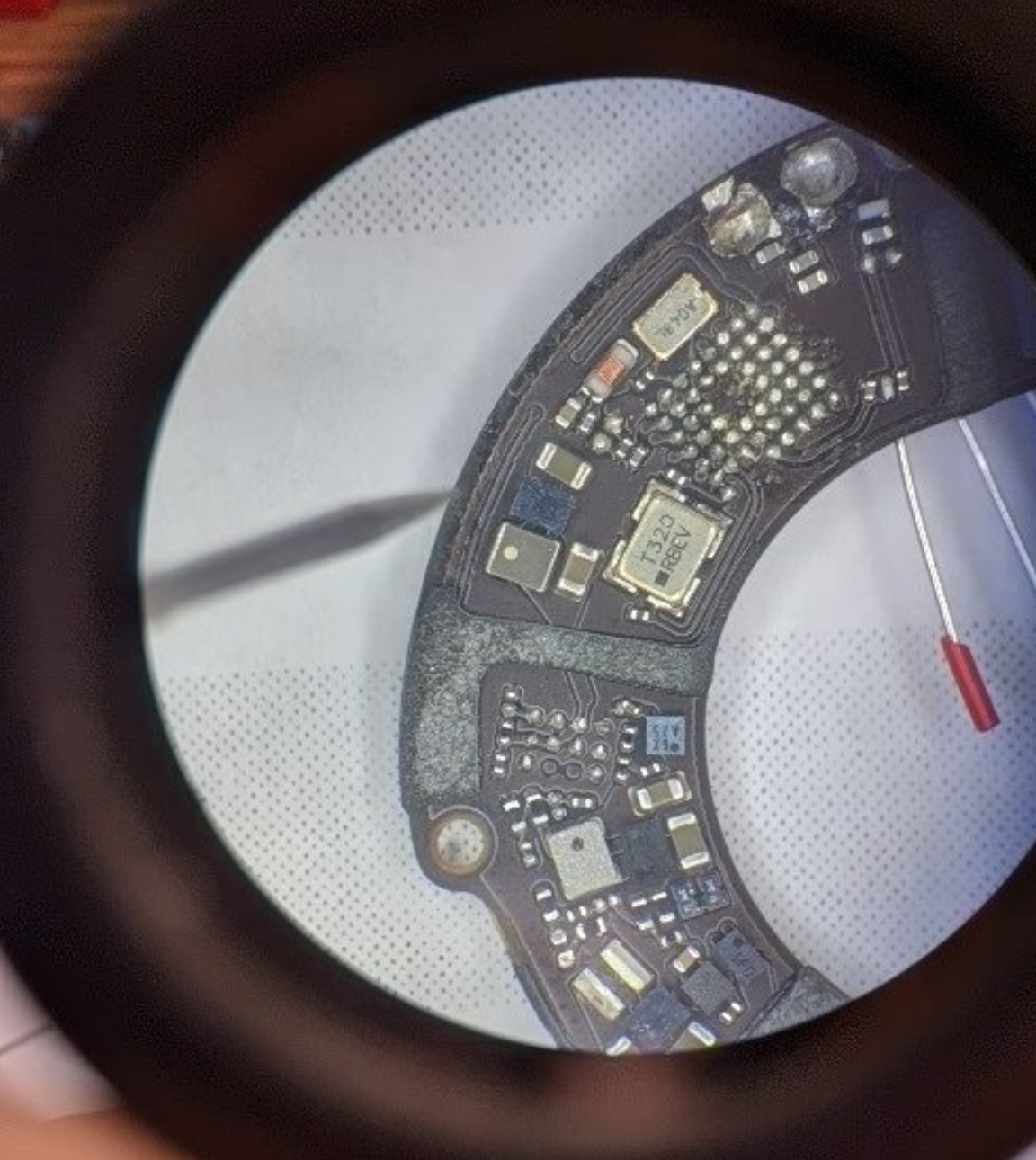
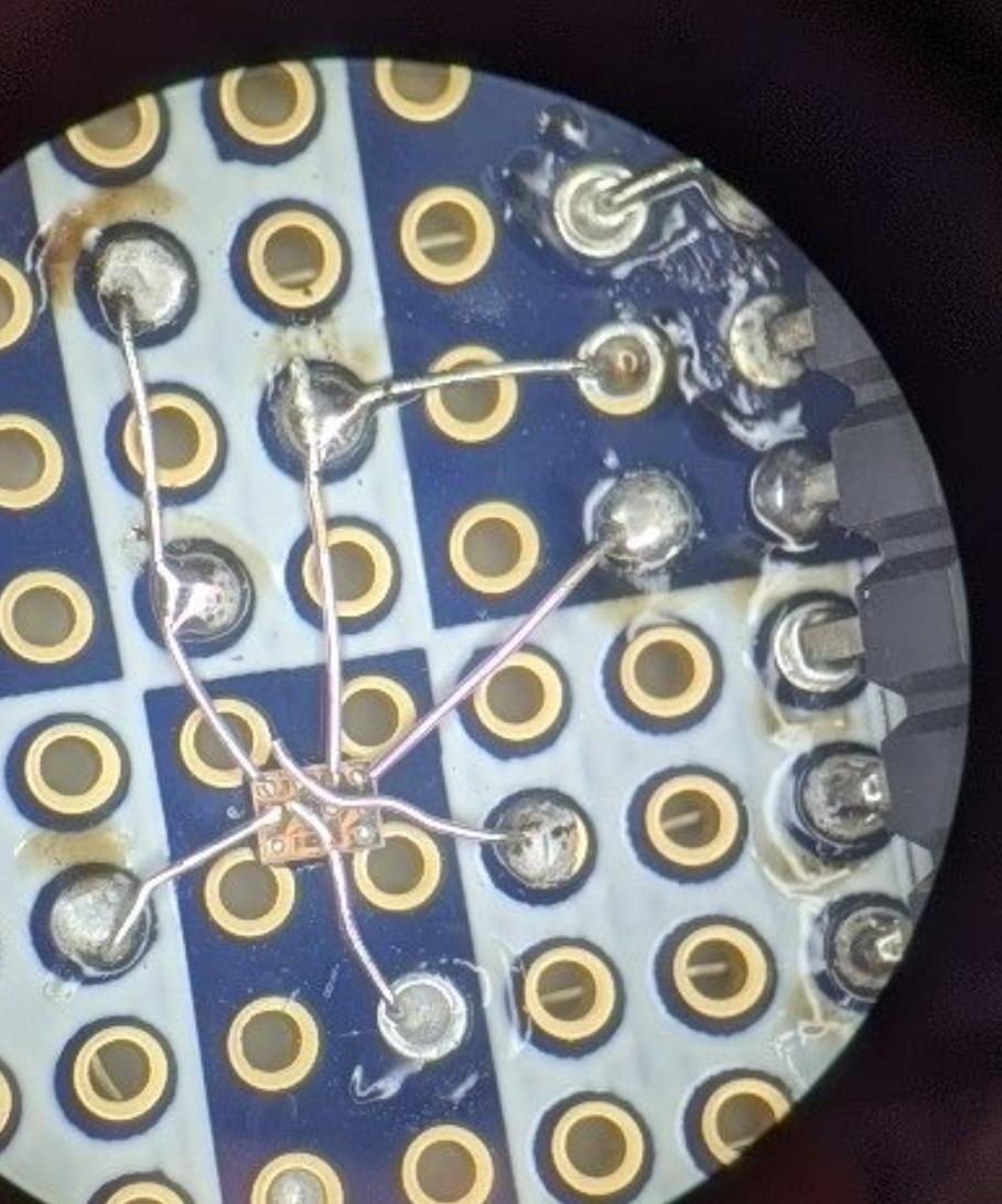
I pulled some of the chips off to investiate any connections between the test points and the chips, using a printed view of the nrf chip while I looked under a microscope as a reference:

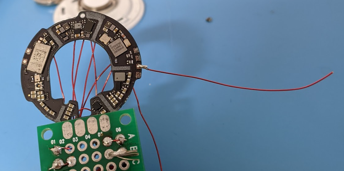
To make probing easier, you can also see how I added some of the test points into wires that then go into my field of view:
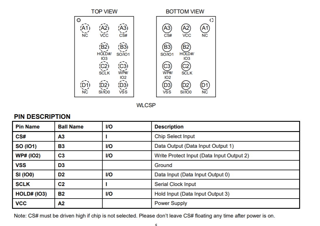
The SPI flash chip had 10 pins on it – it was missing some center pins. Luckily if you check Digikey for SPI flash in WLCSP with 10 pins, there is one single hit: GD25LQ32DLIGR. And from that datasheet you can find the pinout:
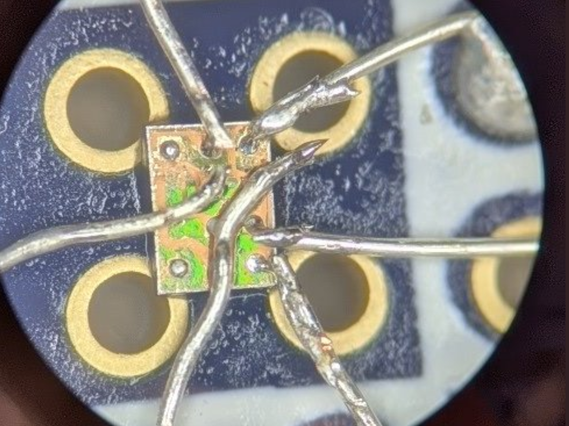
I did a simple dead-bug on the chip to connect up the required pins, here is the center part:
They just run over to some header pins to the right:
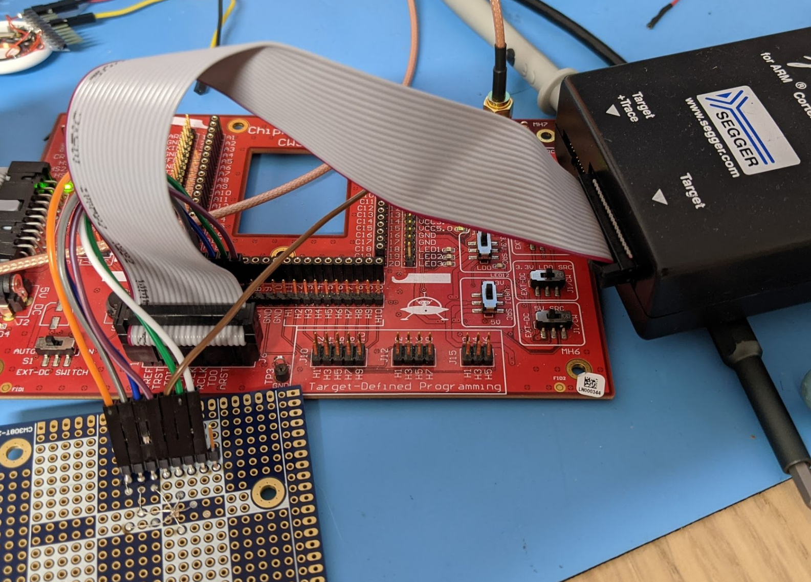
Then you just wire the breakout board up to a SPI reader – I’m using a Segger J-Link due to it’s wide support of various flash chips & very high speed. To provide power I use my own CW308 base board which has a 1.8V regulator:
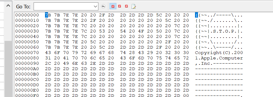
Segger J-Flash SPI detects it as a GD25LQ32C device. I read it twice & verified it, so looks like this worked ok. Apple gives you a good warning at the start of the file:
Interestingly it seems to have a lot of firmware in there – at least the U1 chip firmware, but it looks like nRF firmware as well! I won’t go into that here as wanted to explore how you could talk to this device more easily. But you can see @stacksmashing / @ghidraninja explore this more on a twitter thread:
But if you just want to read/write the SPI flash to play along you can get away with using the test points I linked from the github. All you need is:
- 3.0 to 3.3V to power unit (be sure to power BOTH positive battery tabs – they are NOT connected on the PCB even though you would expect that).
- 1.8V to the SPI power (test point 21)
- SPI connections for the SPI Chip
You’ll need something that supports the GD25LQ32C device to talk to it. Note the nrF is still running here – so it may conflict, but I found the tag is often asleep and our “force power” of the SPI means the nRF isn’t trying to talk to the SPI chip (since the nRF is asleep).
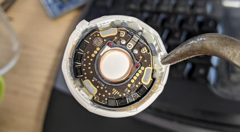
If you want to do fancy emulation stuff (such as with spispy or em100pro-g2), you’ll need to remove the on-board SPI flash. If you want to minimize antenna damage, you can cut through the black plastic as here to pop off the SPI device:
The super-thin PCB quickly heats up, so a short blast of hot air is enough to then pop off the package without damaging anything else. This will leave the antenna for the U1 chip + bluetooth exactly as they were originally.
The repo includes some additional test points including the SWD/SCLK for the nRF chip. But as those are less interesting for intro hardware hacking, I’ve mostly kept to the SPI in this blog post.
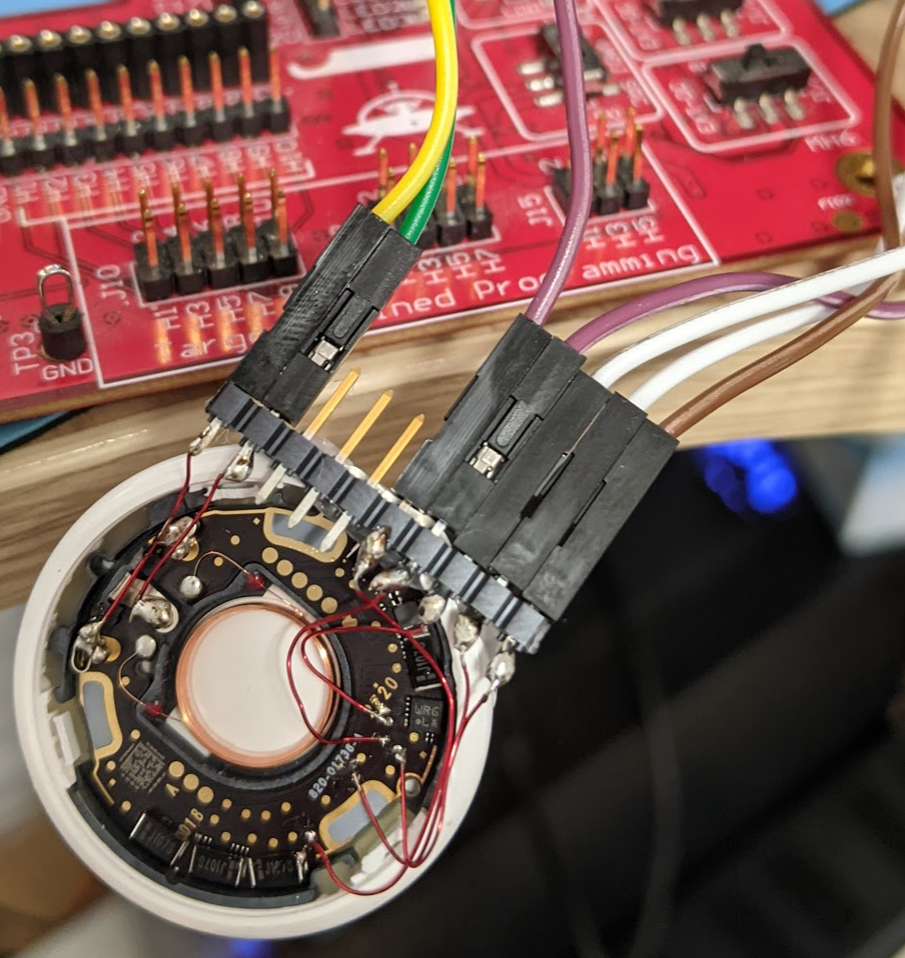
As a bonus – if you want to use the test points w/o soldering onto the test points, I created a simple 3D printed jig. You’ll need to modify it for the test points you want and the pogo pins you are using, I just had a few I was exploring in the default file. The jig when assembled will look something like this:
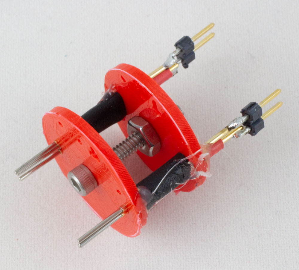
You can find the design files for this in the repo linked earlier. Have fun!
Awesome writeup, love the STOP in the FW ;^)