NOTE: This article appeared in Issue 293 of Circuit Cellar, back in December 2014. I’ve posted it here for your reading pleasure as well. References to previous articles are for Circuit Cellar Issues, as this was originally written for the print publication. This version differs slightly from the print version – this is my own ‘author copy’ version before the Circuit Cellar editing. References to “ProgrammableLogicInPractice.com” are broken for now, but material has been mirrored to the bottom of this page.
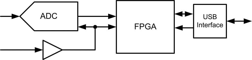
One of the most critical aspects of any FPGA design is where two clock domains meet. The general rule is to avoid this at all costs, but there are situations where it’s unavoidable. A simple situation is shown in Fig. 1, where our system is receiving data from an ADC, but speaking on a common bus. The ADC sample rate is generated from an external source, and might change for specific applications.
A naïve implementation is shown in Fig. 2, where we pay no attention to the two clock domains. By chance it’s very likely that we’re going to attempt to read from the ADC while the data is changing. There are actually two separate issues that pop up here, and I want to give you a more intuitive feeling for both of them.
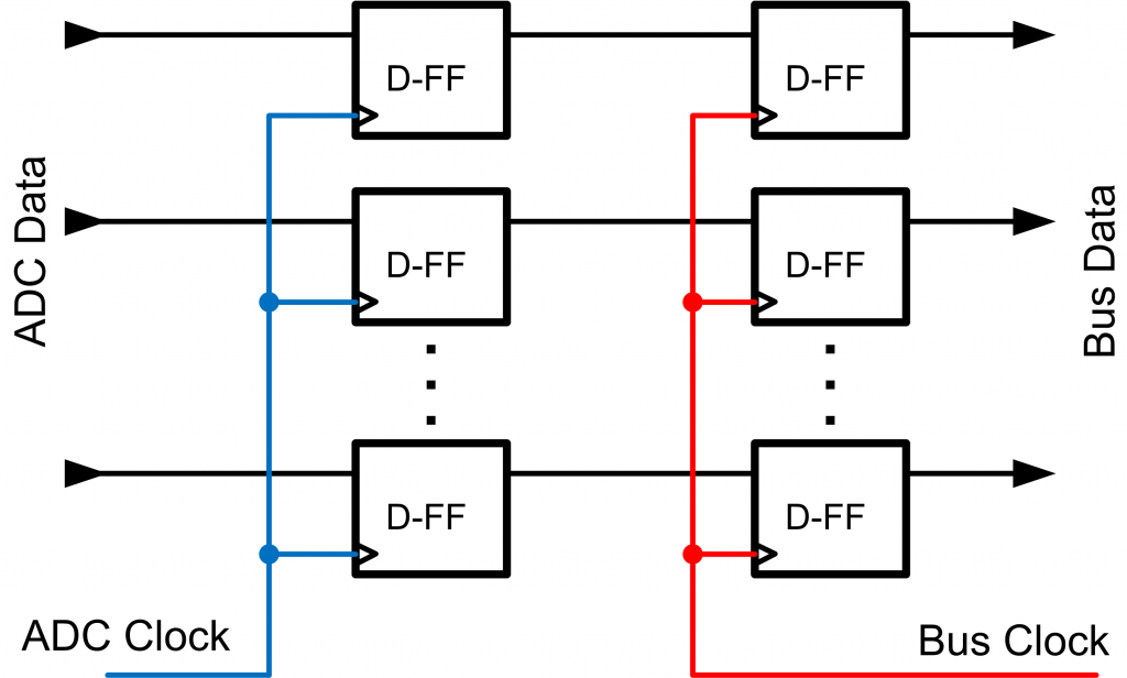
The first is that we might attempt to sample the data in the ‘bus’ clock domain right when the data from the ‘ADC’ clock domain is changing, and we read some incorrect intermediate value. The second is that we might violate setup and hold times of the flip-flops inside our FPGA.
Because this subject is so important, there have been lots written on it. There is a number of online resources, or if you prefer something printed I recommend Chapter 6 of the book Advanced FPGA Design by Steve Kilts. But rather than just rehash this material, I wanted to present to you some real experimental results about failures. Doing this means I’m going to implement a number of designs wrong, and you can see how they fail.
Bus Crossing Experiments
To determine the failure rate of a simple design, I’ve implemented the system shown in Fig. 3. An external clock is used to increment a counter, the value of that counter being read by a system operating from a different clock domain. The previous value of the counter is also kept in another register.
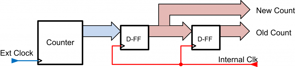
If the system was operating correctly, one would expect that the new value of the counter is the same as the previous value (no count occurred yet), or the previous value plus one (a count occurred). Anything else is flagged as an error, and then the total number of errors is counted, along with total comparisons. From this we can calculate what percentage of reads occurred when invalid data was present. The counters are all large enough that they won’t overflow during the experiment, which would also be flagged as an error.
The internal system clock is operating at 40MHz, and the results are calculated for various external frequencies of 100kHz, 1MHz, and 10MHz. These results are shown in Table 1. Note that exactly as expected the number of failures scales with external frequency, as a faster external frequency simply means more data changes (clock edges), and thus more chances for data to be read at the wrong time.
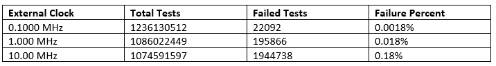
Of special importance you might notice that a substantial number of failures occur even with slow external clocks. When the external clock is 100 kHz we still see a number of failures, even though our system clock is 40 MHz. Thus crossing clock domains is not just something to consider with high-speed designs, but every time you cross clock domains.
Crossing The Smart Way
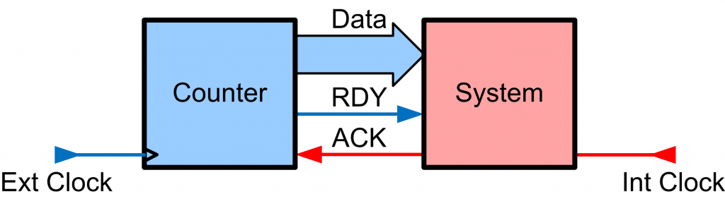
The key to solving this problem is to avoid crossing a number of data lines such as the complete bus, but just to cross a single flag. A better version of this now looks as in Fig. 4, where we also have a ‘Data Ready’ and ‘Acknowledge’ flag. The counter block places new data onto the bus, and keeps that data constant until it has been acknowledged by the other side. Unfortunately even crossing a single line can have trouble as will be explored when we discuss metastability, so we aren’t quite out of the woods yet.
We can avoid the requirement of designing this clock crossing logic by using blocks from our FPGA vendor instead. FPGA vendors provide First In First Out (FIFO) blocks which have different clocks on the read and write ports. The flags are then relative to the proper clock input, i.e. the ‘full’ flag is valid relative to the ‘write’ side.
If we wanted to modify our design to simply insert a FIFO with separate clocks, it would now look as in Fig. 5. This ‘bare minimum’ design uses a FIFO provided by the Xilinx CoreGen tools which has separate clock inputs. The FIFO is setup to write data whenever there is space, and read data whenever it is present. As expected, this change results in no errors using the same test as before.
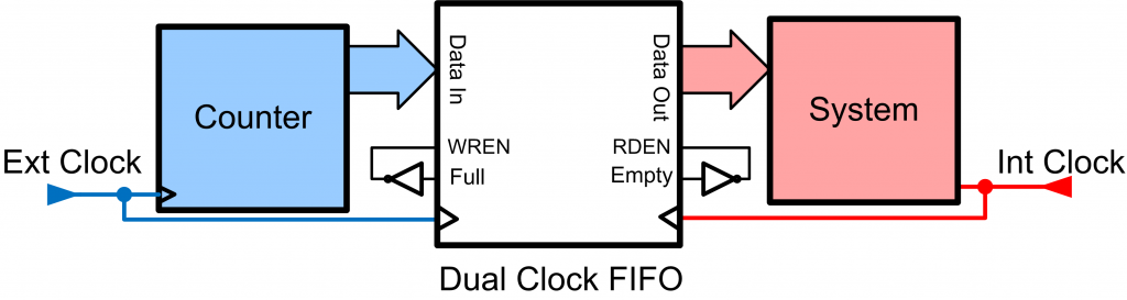
A better design can be had by using the flags properly, such as using the empty flag to determine when new data is present from the counter. You can download these simple files from ProgrammableLogicInPractice.com and experiment yourself on different methods of performing the synchronization.
Metastability Problems
The ‘bus’ problem just mentioned is the most important, since it means when we attempt to read a value from one clock domain we may get completely invalid data. This occurs even for very slow clocks.
There is however another issue that is less obvious, but can have serious ramifications. These are when we violate either the setup or hold time of a flip-flop. The setup time means that the input data to the flip-flip must be stable for some amount of time before the clock edge, and the hold time means the data must remain valid for some amount of time after the clock edge.
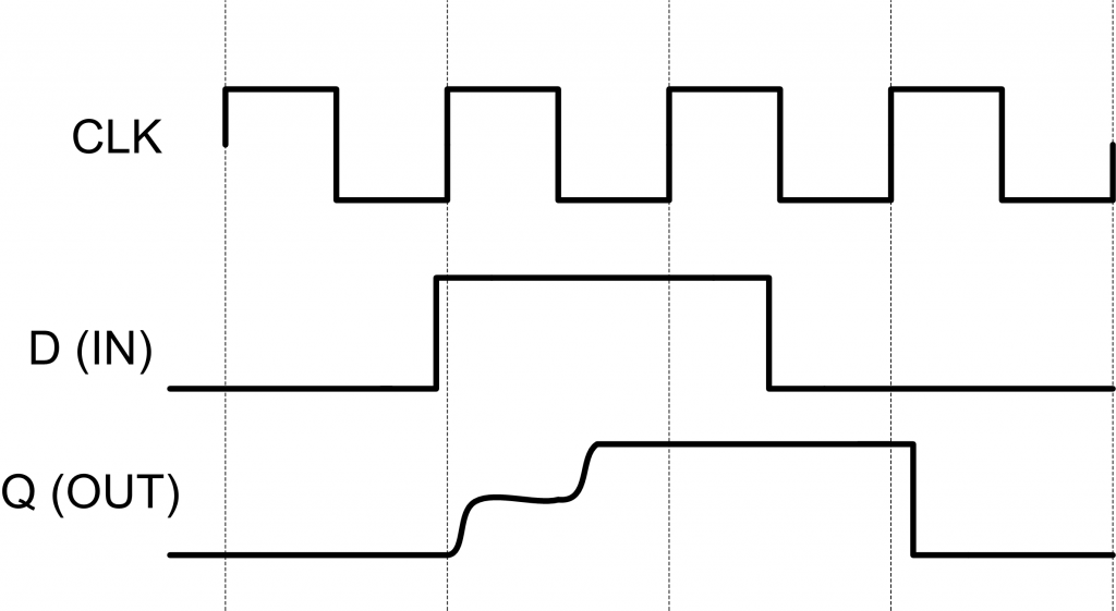
In modern FPGAs (such as the Xilinx Spartan 6 I’m using here) these times are very short, being on the order of 0.5 nS. If they are violated the flip-flop may enter a metastable state, which means the output is at an invalid level, and will eventually resolve to either 0 or 1. This is shown in Fig. 6 – note the metastable state isn’t even a valid logic level. The time it takes for the flip-flop to reach its final state may vary slightly, and is given by a probabilistic measure. Thus if you enter the metastable state it will most likely be resolved in some short period of say 1 nS, but it’s possible (although unlikely) to take say 5 nS. For any design you can thus calculate the Mean Time Between Failure (MTBF) indicating how frequently a metastable state would resulting in a settling time longer than some requirement. Some details are published in appnotes by Xilinx and Altera, although data for more recent families requires contact with a Field Application Engineer (FAE).
If our data is coming from one clock domain, and the internal clock from another, it’s likely we will eventually violate the setup or hold times, and enter this state. The first thing to realize is that there is no incorrect data output occurring – we can’t say the failure is that it should have resolved to ‘0’ but actually resolved to ‘1’. We attempted to sample the data when it was changing, thus it’s not clear what the correct value should have been in this case.
There are two main issues with letting the metastable output be used by the rest of the circuit. The first is that the output of the metastable flip-flop will take longer to propagate than expected, since there is some delay while the output is resolving. This might cause a cascade of failures, since this output can cause other flip-flops to enter a metastable state.
The second is that the invalid logic level representing the metastable state might be read by a ‘1’ in some portions of the circuit and a ‘0’ in other portions, due to small process variations. Thus if the signal is sampled by multiple other entities, completely invalid states could be entered.
Experimenting with Metastability
In order to give you a feel for a metastable circuit, I’ve implemented the block diagram from Fig. 7. The clock can be carefully shifted using a Digital Clock Module (DCM) block in the FPGA, giving me on the order of 100 pS resolution. This is enough to cause the setup time to be violated, and hopefully enter a metastable state.
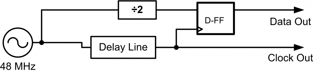
Note we won’t be able to physically see the invalid logic level – I am using an internal flip-flop which is then buffered by the output buffers, thus the output buffer itself will output only a ‘0’ or a ‘1’. We will however be able to see the longer time it takes to resolve a metastable state.
Operating correctly, the output of the flip-flop would be a change on every rising edge of the 48 MHz clock. Once we start violating the setup time this won’t happen – sometimes the flip-flop will latch the new value (i.e. changing the output), sometimes the flip-flop will latch the old value (i.e. not changing the output).
Initially the system is operating correctly, as in the diagram from Fig. 8A, which uses a persistence vision mode in the oscilloscope to plot hundreds of traces on-top of each other. The most common path taken is shown in red, and as expected the output of the flip-flop is always changing on the rising edge of the clock. This figure is taken for a Spartan 6 LX75 device with the clock running at 48 MHz. The core voltage (VCCINT) is 1.2V, although this figure looks almost identical even if I drop the core voltage to 0.7V (well below the allowed range from the datasheet). I’ll be using this lower core voltage to exaggerate the metastable effect.
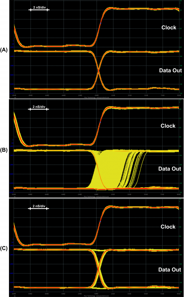
Next, I’ll force the flip-flop to enter metastability. To give you a more obvious figure I’ve dropped the core voltage of the FPGA to 0.7V (again this is BELOW the normal minimum voltage of 1.14V for VCCINT). In Fig. 8B you can see it was taking almost 5nS for the output to resolve in some cases, although as you can see it was more common for a quicker resolution. But going back to a real-life case let’s look at when the core voltage is set to 1.2V. The results in Fig. 8C aren’t so dramatic looking, but you can see the additional time required for the metastable state to resolve.
You can observe some of this in the following video:
Solving Metastability
The most classic solution to this problem in shown in Fig. 9, which uses two D flip-flops in a row. If the first flip-flop enters a metastable state, it should be resolved before the second flip-flop samples the output. For most reasonable clock speeds and recent devices this will be true, although there is always still a possibility of the second flip-flop entering a metastable state. The complete system is still characterized by the MTBF, and in some applications three or more flip-flops might be chained to increase the MTBF.
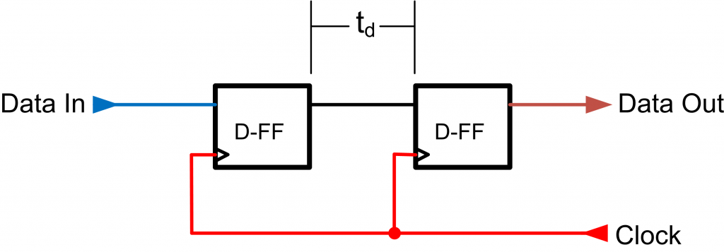
Just adding two flip-flops as in Fig. 9 isn’t enough – you must ensure you are implementing the circuit you intend, not what the synthesis tools guess you are doing. In particular this circuit looks like a shift register, thus it may insert a shift-register primitive which doesn’t have the desired metastability characteristics. In addition you may need to constrain the path between the flip-flops, since the tools don’t know that you actually want the shortest possible path between those flip-flops. The tools may assume you are only constrained by the clock period, but in reality you want an even faster route, since the objective is to provide enough ‘slack time’ for the metastable output to resolve to a final value.
The circuit which safely crosses clock domains is called a synchronizer. Different FPGA vendors and families have different best practices about how to implement this.
Your best resource is to check for app-notes specific to your FPGA family, and then branch out into general best practices for your vendor (lacking family-specific information). I’ll post some links on ProgrammableLogicInPractice.com for such information on Xilinx Spartan 6 devices, although as mentioned the book Advanced FPGA Design is a good starting point. Xilinx has an older app-note, XAPP094 which provide some detail, with measurements for more recent devices available only on request from the FAE. Altera provides app-note 42 for some basic details, which also links to specifics of implementing synchronizers using the Quartus-II software.
Staying Stable
Hopefully you found some real-world examples of what synchronization failures and metastability looks like useful. Whilst lots has been written on the issue, I’m hoping the practical results from this article shows you the problem clearly, and how you can experiment yourself with solutions. Understanding the real problem will help you make better design decisions – there’s no silver bullet for every situation, and by keeping some of these experiments in mind you might find it easier to base your design on solving real problems, not textbook suggestions.
See below for the FPGA project files.
REFERENCES / MORE INFORMATION
Altera, App-Note 42: ftp://ftp.altera.com/pub/lit_req/document/an/an042.pdf
Xilinx, App-Note 94: http://www.xilinx.com/support/documentation/application_notes/xapp094.pdf
Steve Kilts,Advanced FPGA Design
Lecure 07 of MIT Class 6.004: http://6004.csail.mit.edu/currentsemester/
Ran Ginosar, Metastability and Synchronizers: A Tutorial: http://webee.technion.ac.il/~ran/papers/MetastabilitySynchronizersTutorialIEEEDT2011.pdf
December 2014 Post on ProgrammableLogicInPractice.com [No Longer Available]
REFERENCE FILES