I recently got my Glasgow device, which is a rather impressive piece of tech. I followed the Windows installation instructions and it “Just Worked”, including installing the toolchain! On one computer I needed to use Zadig to force the driver to be libusbK, but on another Windows computer it wasn’t needed. In this blog post, I’m going to explore a parallel NAND device that I wanted to dump, and find out how well Glasgow works.
About Parallel NAND & Mounting
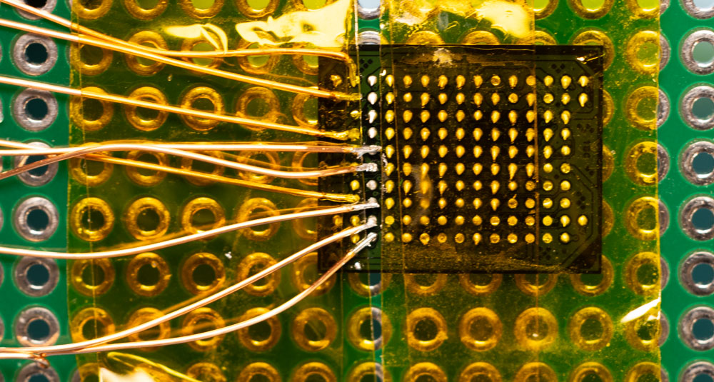
The first step was mounting the FLASH chip. The chip in question (MT29F4G08ABBDA3W) is a dual-package DDR and NAND flash device. I did this dead-bug style, using a pinout map I printed out and mirrored to make it easier for me to tack wires onto each one:
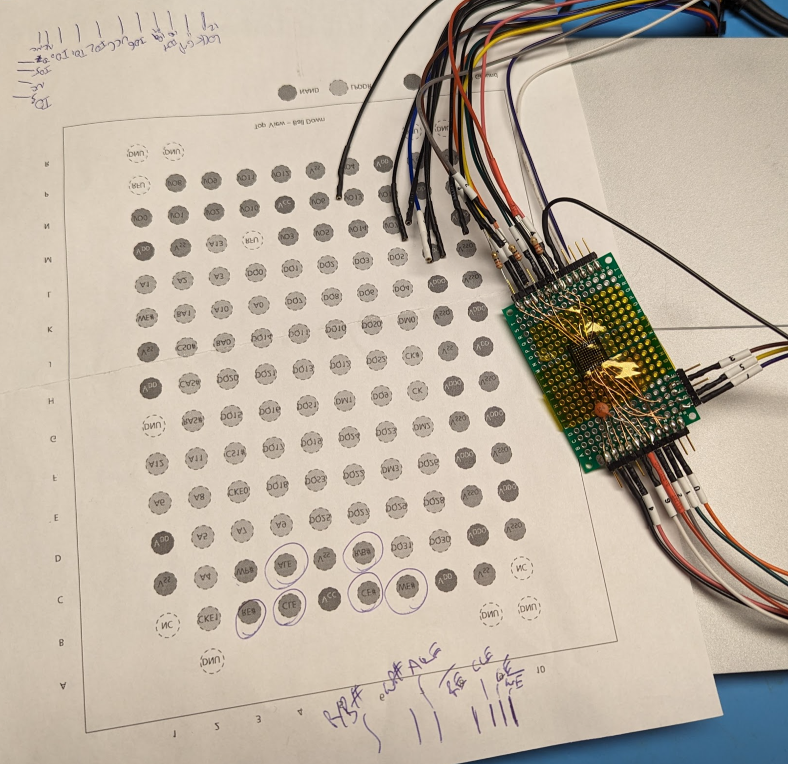
For each row I used kaptop tape to hold down the previous row, so I didn’t have to worry about knocking previously soldered wires off. I also only connected one GND & VCC pin – the NAND portion only had a couple VCC pins anyway, but it was even easier if I could only connect a single one. Here’s a photo of this part-way. Notice I only expose a single row of pads to make it easier to solder to only the right pads. Once a row is done I cover it with kapton tape, which protects it from the next layer of soldering, in addition to giving it more mechanical strength. The wire is an enamel coated wire with a low temperature insulation that will melt off soldering iron heat.
In Glasgow you’ll see reference to Open NAND Flash Interface (ONFI). If you do a search of the datasheet ONFI might not show up, but if you check the datasheet you’ll see that it supports ONFI as this is part of the identification:
Glasgow parallel NAND support
As described above, these devices are described as ONFI. I used the glasgow memory-onfi command. Here is the help output showing everything you’ll need to use it:
usage: glasgow run memory-onfi [-h] [--port SPEC] [--pins-io SET] [--pin-cle NUM] [--pin-ale NUM] [--pin-re NUM] [--pin-we NUM] [--pin-r-b NUM] [--pins-ce SET]
                               (-V [VOLTS] | -M | --keep-voltage) [-c CHIP] [-P SIZE] [-S SIZE] [-B SIZE]
                               OPERATION ...

This applet is PREVIEW QUALITY and may CORRUPT DATA or have missing features. Use at your own risk.

Identify, read and write memories compatible with ONFI NAND Flash memory. The applet roughly follows the ONFI 1.0 specification, but tolerates the very common non-ONFI-
compliant memories by gracefully degrading autodetection of memory functionality.

Only the asynchronous NAND interface is supported. All R/B# pins should be tied together, and externally pulled up. All CE# pins must be either connected or pulled high to
avoid bus contention; for unidentified devices, this means all 4 CE# pins available on the package.

The NAND Flash command set is not standardized in practice. This applet uses the following commands when identifying the memory:

  * Cmd 0xFF: Reset (all devices)
  * Cmd 0x90 Addr 0x00: Read ID, JEDEC Manufacturer and Device (all devices)
  * Cmd 0x90 Addr 0x20: Read ID, ONFI Signature (ONFI and some non-ONFI devices)
  * Cmd 0xEC: Read Parameter Page (ONFI only)

If the memory doesn't respond or gives invalid response to ONFI commands, it can still be used, but the array parameters need to be specified explicitly.

The applet use the following commands while reading and writing data:

  * Cmd 0x70: Read Status (all devices)
  * Cmd 0x00 Addr Col1..2,Row1..3 Cmd 0x30: Read (all devices)
  * Cmd 0x60 Addr Row1..3 Cmd 0xD0: Erase (all devices)
  * Cmd 0x80 Addr Col1..2,Row1..3 [Cmd 0x85 Col1..2]+ Cmd 0x10: Page Program (all devices)

positional arguments:
  OPERATION
    identify                identify device using ONFI parameter page
    read                    read data and spare contents for a page range
    program                 program data and spare contents for a page range
    erase                   erase any blocks containing a page range

options:
  -h, --help                show this help message and exit
  -P SIZE, --page-size SIZE
                            Flash page (without spare) size, in bytes (default: autodetect)
  -S SIZE, --spare-size SIZE
                            Flash spare size, in bytes (default: autodetect)
  -B SIZE, --block-size SIZE
                            Flash block size, in pages (default: autodetect)

build arguments:
  --port SPEC               bind the applet to port SPEC (default: AB)
  --pins-io SET             bind the applet I/O lines 'io' to pins SET (default: 0,1,2,3,4,5,6,7)
  --pin-cle NUM             bind the applet I/O line 'cle' to pin NUM (default: 8)
  --pin-ale NUM             bind the applet I/O line 'ale' to pin NUM (default: 9)
  --pin-re NUM              bind the applet I/O line 're' to pin NUM (default: 10)
  --pin-we NUM              bind the applet I/O line 'we' to pin NUM (default: 11)
  --pin-r-b NUM             bind the applet I/O line 'r_b' to pin NUM (default: 12)
  --pins-ce SET             bind the applet I/O lines 'ce' to pins SET (default: 13,14)

run arguments:
  -V [VOLTS], --voltage [VOLTS]
                            set I/O port voltage explicitly
  -M, --mirror-voltage      sense and mirror I/O port voltage
  --keep-voltage            do not change I/O port voltage
  -c CHIP, --chip CHIP      select chip connected to CE# signal CHIP (one of: 1..4, default: 1)
The important part is the pin numbering. You can change where pins connect to, but since I was just wiring my board up using fly wires, I followed their suggested example pins. Note that pin 8 = B0, 9 = B1, etc in this example. I also had wired out the LOCK pin, which the datasheet says you can just ignore.
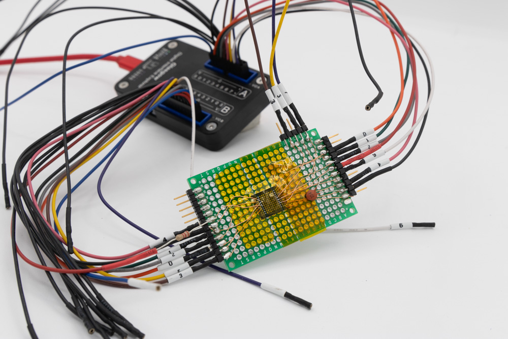
Watch the RB pin – you need a pull-up on this pin, as it’s open-drain by default. I used a 2.2K resistor and pulled it up using the VCC connection from the B port. At this point my setup looks something like this:
Nice! Now with great hope in our heart we run the identify command. I’ll save you some space and tell you to also include the verbose output, like this: glasgow -v run memory-onfi -V 1.8 identify
$ glasgow -v run memory-onfi -V 1.8 identify

D: glasgow.device.hardware: found revC3 device with serial C3-20240303T140525Z
D: glasgow.applet.memory.onfi: claimed pipe P and port(s) A, B
D: glasgow.applet.memory.onfi: adding reset register at address 0x00
D: glasgow.applet.memory.onfi: assigning pin 'cle' to device pin B0
D: glasgow.applet.memory.onfi: assigning pin 'ale' to device pin B1
D: glasgow.applet.memory.onfi: assigning pin 're' to device pin B2
D: glasgow.applet.memory.onfi: assigning pin 'we' to device pin B3
D: glasgow.applet.memory.onfi: assigning pin 'r_b' to device pin B4
D: glasgow.applet.memory.onfi: assigning pin set 'io' to device pins A0, A1, A2, A3, A4, A5, A6, A7
D: glasgow.applet.memory.onfi: assigning pin set 'ce' to device pins B5, B6
D: glasgow.target.toolchain: using toolchain 'builtin' (yosys 0.39.0.0.post694, nextpnr-ice40 0.7.0.0.post519, icepack 0.7.0.0.post519)
I: glasgow.device.hardware: generating bitstream ID 18adf47dd70eb39c986fdd271f431495
D: glasgow.target.hardware: bitstream ID 18adf47dd70eb39c986fdd271f431495 is cached
I: glasgow.cli: running handler for applet 'memory-onfi'
W: glasgow.cli: applet 'memory-onfi' is PREVIEW QUALITY and may CORRUPT DATA
I: glasgow.applet.memory.onfi: port(s) A, B voltage set to 1.8 V
D: glasgow.applet.memory.onfi: port(s) A, B pull resistors disabled
D: glasgow.applet.memory.onfi: ONFI: select chip=0
D: glasgow.applet.memory.onfi: ONFI: reset
D: glasgow.applet.memory.onfi: ONFI: command=0xff
D: glasgow.applet.memory.onfi: ONFI: r/b wait
D: glasgow.applet.memory.onfi: ONFI: select chip=1
D: glasgow.applet.memory.onfi: ONFI: reset
D: glasgow.applet.memory.onfi: ONFI: command=0xff
D: glasgow.applet.memory.onfi: ONFI: r/b wait
D: glasgow.applet.memory.onfi: ONFI: select chip=0
D: glasgow.applet.memory.onfi: ONFI: read ID addr=0x00
D: glasgow.applet.memory.onfi: ONFI: command=0x90 address=<00>
D: glasgow.applet.memory.onfi: ONFI: read data=<2cac>
I: glasgow.applet.memory.onfi: JEDEC manufacturer 0x2c (Micron Technology) device 0xac
D: glasgow.applet.memory.onfi: ONFI: read ID addr=0x00
D: glasgow.applet.memory.onfi: ONFI: command=0x90 address=<00>
D: glasgow.applet.memory.onfi: ONFI: read data=<2cac9015>
I: glasgow.applet.memory.onfi: ID signature: 2c ac 90 15
D: glasgow.applet.memory.onfi: ONFI: read ID addr=0x20
D: glasgow.applet.memory.onfi: ONFI: command=0x90 address=<20>
D: glasgow.applet.memory.onfi: ONFI: read data=<4f4e4649>
D: glasgow.applet.memory.onfi: ONFI: read parameter page copies=3
D: glasgow.applet.memory.onfi: ONFI: command=0xec address=<00>
D: glasgow.applet.memory.onfi: ONFI: r/b wait
D: glasgow.applet.memory.onfi: ONFI: read data=<4f4e4649020018003f000000000000000000000000000000000000000000004d4943524f4e2020202020204d543239463447303841424244413357202020202c... (768 bytes total)>
W: glasgow.applet.memory.onfi: invalid ONFI parameter page: integrity checks failed on all redundant pages
E: glasgow.applet.memory.onfi: cannot identify non-ONFI device
Hmm, what happened? That data looks “pretty valid”, but not quite there? Lets dig into Glasgow to see how we can get more information about what happened.
Modifying Glasgow Applets
After following the Glasgow instructions, I had my copy of glasgow cloned from git into a directory. But I was running Glasgow at the command line just like any other tool. Luckily because Glasgow was installed in “editable” mode, it will use my cloned files to run my commands. So any changes we make to the source Python are reflected immediately in our tool.
I’ll make a few changes to two files to help with my debugging. If you want to follow along, the files for reference are (GitHub links):
https://github.com/GlasgowEmbedded/glasgow/blob/main/software/glasgow/applet/memory/onfi/__init__.py
https://github.com/GlasgowEmbedded/glasgow/blob/main/software/glasgow/protocol/onfi.py
It’s the latter one that includes the CRC check that is failing. At line 101 at the linked checkout (may have changed on current main), there is a CRC check. I forced it to print the *entire* failing CRC by adding lines 103-105:
101:            if crc_expected == crc_actual:
102:                break
103:            else:
104:                print("%x != %x"%(crc_actual, crc_expected))
105:                print(" ".join(["%02x"%d for d in data[:254]]))
This gave me the following debug output:
4e2020202020204d543239463447303841424244413357202020202c... (768 bytes total)>
ef01 != 4f0c
4f 4e 46 49 02 00 18 00 3f 00 00 00 00 00 00 00 00 00 00 00 00 00 00 00 00 00 00 00 00 00 00 4d 49 43 52 4f 4e 20 20 20 20 20 20 4d 54 32 39 46 34 47 30 38 41 42 42 44 41 33 57 20 20 20 20 2c 00 00 00 00 00 00 00 00 00 00 00 00 00 00 00 00 08 00 00 40 00 00 02 00 00 10 00 40 00 00 00 00 10 00 00 01 23 01 50 00 01 05 01 00 00 04 00 04 01 0e 00 00 00 00 00 00 00 00 00 00 00 00 00 0a 1f 00 1f 00 58 02 b8 0b 19 00 64 00 00 00 00 00 00 00 00 00 00 00 00 00 00 00 00 00 00 00 00 00 00 00 00 01 00 01 00 00 02 04 80 01 81 04 01 02 01 0a 00 00 00 00 00 00 00 00 00 00 00 00 00 00 00 00 00 00 00 00 00 00 00 00 00 00 00 00 00 00 00 00 00 00 00 00 00 00 00 00 00 00 00 00 00 00 00 00 00 00 00 00 00 00 00 00 00 00 00 00 00 00 00 00 00 00 00 00 00 00 00 00 00 00 00 72
99ec != 4e4f
4e 46 49 02 00 18 00 3f 00 00 00 00 00 00 00 00 00 00 00 00 00 00 00 00 00 00 00 00 00 00 4d 49 43 52 4f 4e 20 20 20 20 20 20 4d 54 32 39 46 34 47 30 38 41 42 42 44 41 33 57 20 20 20 20 2c 00 00 00 00 00 00 00 00 00 00 00 00 00 00 00 00 08 00 00 40 00 00 02 00 00 10 00 40 00 00 00 00 10 00 00 01 23 01 50 00 01 05 01 00 00 04 00 04 01 0e 00 00 00 00 00 00 00 00 00 00 00 00 00 0a 1f 00 1f 00 58 02 b8 0b 19 00 64 00 00 00 00 00 00 00 00 00 00 00 00 00 00 00 00 00 00 00 00 00 00 00 00 01 00 01 00 00 02 04 80 01 81 04 01 02 01 0a 00 00 00 00 00 00 00 00 00 00 00 00 00 00 00 00 00 00 00 00 00 00 00 00 00 00 00 00 00 00 00 00 00 00 00 00 00 00 00 00 00 00 00 00 00 00 00 00 00 00 00 00 00 00 00 00 00 00 00 00 00 00 00 00 00 00 00 00 00 00 00 00 00 00 00 72 0c
7546 != 464e
46 49 02 00 18 00 3f 00 00 00 00 00 00 00 00 00 00 00 00 00 00 00 00 00 00 00 00 00 00 4d 49 43 52 4f 4e 20 20 20 20 20 20 4d 54 32 39 46 34 47 30 38 41 42 42 44 41 33 57 20 20 20 20 2c 00 00 00 00 00 00 00 00 00 00 00 00 00 00 00 00 08 00 00 40 00 00 02 00 00 10 00 40 00 00 00 00 10 00 00 01 23 01 50 00 01 05 01 00 00 04 00 04 01 0e 00 00 00 00 00 00 00 00 00 00 00 00 00 0a 1f 00 1f 00 58 02 b8 0b 19 00 64 00 00 00 00 00 00 00 00 00 00 00 00 00 00 00 00 00 00 00 00 00 00 00 00 01 00 01 00 00 02 04 80 01 81 04 01 02 01 0a 00 00 00 00 00 00 00 00 00 00 00 00 00 00 00 00 00 00 00 00 00 00 00 00 00 00 00 00 00 00 00 00 00 00 00 00 00 00 00 00 00 00 00 00 00 00 00 00 00 00 00 00 00 00 00 00 00 00 00 00 00 00 00 00 00 00 00 00 00 00 00 00 00 00 00 72 0c 4f
What’s going on here? While the issue is that we’ve actually *dropped* a byte. In the first sequence of 00’s it is one 00 byte short! If you hack the source to insert an extra zero byte at that location, it will “just work”. How do we actually fix it though?
One thing you could try is to modify the Glasgow applet to increase the wait cycles, you can see right here. If you change that constant and rerun glasgow, you’ll see a FPGA build happen. It’s amazing how quickly changes in “RTL” become real, and shows that there is a lot of power hidden in this system. But ultimately that won’t do much, because the root cause isn’t something you can easily fix in RTL, but related to my physical board.
Adding Termination Resistors
The fact we were missing bytes was a bit of a red flag. The most likely scenario here is that the NAND chip actually output two bytes at some point, which suggested to me it was seeing two transitions on the read or write flags. Remember the NAND stuff is all asynchronous so if there is toggling on the lines it will do the reads! And because my breakout board was so hacky it would be hardy surprising!
Scoping the WE pin in combination with a random data pin (to also check timing on the flag transition) suggested this was the case. Check out how much ringing we are seeing:
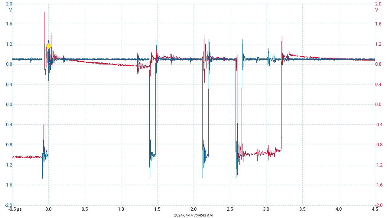
Not good! Wait cycles won’t help us here, because it’s the high slew rate in combination with our long leads & very poorly constructed breakout board that is probably contributing to this. We need to slow down the slew rate, and the easiest way is some series resistors.
As @Whitequark pointed out, there are some in there already (33R)! So most of the time you won’t need them, but I found my *extremely poor quality* breakout had…. trouble. I’m not positive if the ringing is truly the root cause or it masked something else, either way it mostly worked adding additional ones right at my breakout.
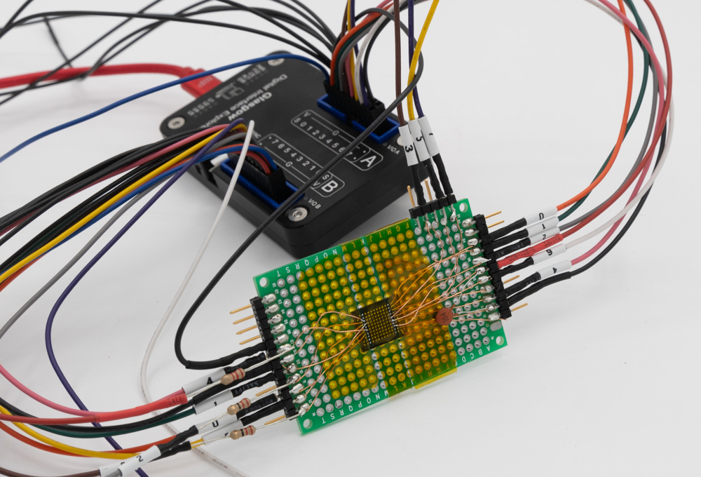
Now I’m too lazy to add resistors to all the pins, so I just added them to the ones I thought would matter: the read & write flag pins, WE and RE. It’s those pins that if they have extra transitions will cause extra bytes to be clocked in (or out) of the device, which would mean bad things are going to happen to our device! Here’s how the series resistors look now, there is just two resistors connected instead of directly to the glasgow on two pins:
Running identify is now much more satisfying:
I: glasgow.device.hardware: device already has bitstream ID 18adf47dd70eb39c986fdd271f431495
I: glasgow.cli: running handler for applet 'memory-onfi'
W: glasgow.cli: applet 'memory-onfi' is PREVIEW QUALITY and may CORRUPT DATA
I: glasgow.applet.memory.onfi: port(s) A, B voltage set to 1.9 V
I: glasgow.applet.memory.onfi: JEDEC manufacturer 0x2c (Micron Technology) device 0xac
I: glasgow.applet.memory.onfi: ID signature: 2c ac 90 15
I: glasgow.applet.memory.onfi: ONFI revision 1.0
I: glasgow.applet.memory.onfi: ONFI manufacturer information:
I: glasgow.applet.memory.onfi:                    JEDEC ID: 0x2c (Micron Technology)
I: glasgow.applet.memory.onfi:                manufacturer: MICRON
I: glasgow.applet.memory.onfi:                       model: MT29F4G08ABBDA3W
I: glasgow.applet.memory.onfi:                   date code: (not specified)
I: glasgow.applet.memory.onfi: Features:
I: glasgow.applet.memory.onfi:              data bus width: 8-bit
I: glasgow.applet.memory.onfi:        multi-LUN operations: no
I: glasgow.applet.memory.onfi:     block programming order: sequential
I: glasgow.applet.memory.onfi:      interleaved operations: yes
I: glasgow.applet.memory.onfi:        odd-to-even copyback: yes
I: glasgow.applet.memory.onfi: Optional commands:
I: glasgow.applet.memory.onfi:          Page Cache Program: yes
I: glasgow.applet.memory.onfi:   Read Cache (Enhanced/End): yes
I: glasgow.applet.memory.onfi:            Get/Set Features: yes
I: glasgow.applet.memory.onfi:        Read Status Enhanced: yes
I: glasgow.applet.memory.onfi:       Copyback Program/Read: yes
I: glasgow.applet.memory.onfi:              Read Unique ID: yes
I: glasgow.applet.memory.onfi: Memory organization:
I: glasgow.applet.memory.onfi:                   page size: 2048 + 64 bytes
I: glasgow.applet.memory.onfi:           partial page size: 512 + 16 bytes
I: glasgow.applet.memory.onfi:                  block size: 64 pages
I: glasgow.applet.memory.onfi:                    LUN size: 4096 blocks; 262144 pages
I: glasgow.applet.memory.onfi:                 target size: 1 LUNs; 4096 blocks; 262144 pages
I: glasgow.applet.memory.onfi:              address cycles: 3 row, 2 column
I: glasgow.applet.memory.onfi:               bits per cell: 1
I: glasgow.applet.memory.onfi:          bad blocks per LUN: 80 (maximum)
I: glasgow.applet.memory.onfi:             block endurance: 100000 cycles (maximum)
I: glasgow.applet.memory.onfi:           guaranteed blocks: 1 (at target beginning)
I: glasgow.applet.memory.onfi:  guaranteed block endurance: 0 cycles
I: glasgow.applet.memory.onfi:           programs per page: 4 (maximum)
I: glasgow.applet.memory.onfi:          ECC correctability: 4 bits (maximum, per 512 bytes)
I: glasgow.applet.memory.onfi: Electrical parameters:
I: glasgow.applet.memory.onfi:         I/O pin capacitance: 10 pF
I: glasgow.applet.memory.onfi:                timing modes: 0, 1, 2, 3, 4
I: glasgow.applet.memory.onfi:  program cache timing modes: 0, 1, 2, 3, 4
I: glasgow.applet.memory.onfi:           page program time: 600 us (maximum)
I: glasgow.applet.memory.onfi:            block erase time: 3000 us (maximum)
I: glasgow.applet.memory.onfi:              page read time: 25 us (maximum)
I: glasgow.applet.memory.onfi:    change column setup time: 100 us (minimum)
Check that “LUN Size”, and note there is a total of 262144 pages. We’ll need that number when we go to dump out the entire flash. But first, let’s check if it’s actually working well (or well enough at least).
Dumping Reliably
Now we’ll run a dump of 1000 pages four times in a row, like this:
glasgow run memory-onfi -V 1.8 read 0 1000 test001.bin
glasgow run memory-onfi -V 1.8 read 0 1000 test002.bin
glasgow run memory-onfi -V 1.8 read 0 1000 test003.bin
glasgow run memory-onfi -V 1.8 read 0 1000 test004.bin
Then run a diff between the files to check if they are the same (or not). In my case I still had some issues, and it still looked like occasionally dropping bytes (I used the 010 Editor compare mode to see this, as it does a good job of showing inserted/skipped bytes). Rather than fix the SI issues (the right answer) I hacked up some software. To do this, I modified the applet around line 709 to look like this:
            while count > 0:
                self.logger.info("reading page (row) %d", row)
                chunk = await onfi_iface.read(column=0, row=row, length=page_size + spare_size)
                chunk1 = await onfi_iface.read(column=0, row=row, length=page_size + spare_size)
                chunk2 = await onfi_iface.read(column=0, row=row, length=page_size + spare_size)
                chunk3 = await onfi_iface.read(column=0, row=row, length=page_size + spare_size)

                if chunk == chunk1 == chunk2 == chunk3:
                    pass
                else:
                    self.logger.info("oops, multi-read failed, retrying...")
                    continue
I should point out this can easily fail, since the error cases aren’t random but seem to be based on e.g., the data pattern resulting in more ringing. In my case I didn’t need a clean dump but wanted to check if root password were constant or not between units, so I was happy enough to accept some corrupted data as a risk. You may want to experiment more with the series resistors, decoupling caps, or connecting more of the VCC/GNDs to improve your experience!
glasgow run memory-onfi -V 1.8 read 0 262144 flash_dump.binAnd finally you can work through it with binwalk. In my case though I didn’t need such fancy stuff, just a simple:
strings flash_dump.bin | grep '\$1\$'
Dumped out the hash of the root password. I did try a few different dumps to reduce the chance my one section was corrupted! But I’m going to combine this with some JTAG work to access the FLASH a second way, a topic for another blog post.
Rev April 14/2024 Edit: Added note from Whitequark about series termination resistors in all the lines, hopefully you won’t normally need to add them.