I recently got my Glasgow device, which is a rather impressive piece of tech. I followed the Windows installation instructions and it “Just Worked”, including installing the toolchain! On one computer I needed to use Zadig to force the driver to be libusbK, but on another Windows computer it wasn’t needed. In this blog post, I’m going to explore a parallel NAND device that I wanted to dump, and find out how well Glasgow works.
Continue reading Dumping Parallel NAND with GlasgowCategory: Hardware Hacking
RECON 2023: Adventures of My Oven (Pinocchio) with ChipWhisperer
At RECON2023 I gave a talk about reverse engineering my Samsung Oven. This blog post has slides & links to information, with more to come! You can get a copy of the slides below:
Oven-Specific Stuff: https://github.com/colinoflynn/samsung-ovens-deconstructed
Python Loader for TMP91 Series: https://github.com/colinoflynn/pytoshload
Resource CD for TLCS900: https://github.com/colinoflynn/Toshiba-TLCS-900-L-Resources
New England Hardware Security Day 2022 Talk
On April 1st, 2022 I gave a “workshop” at New England Hardware Security Day. This blog post is a quick summary of some of the links to recreate my demos from that talk. Here is a copy of the slides if you’d like them:
DFA on Raspberry Pi with PicoEMP

This demo is pretty simple – it recreates the classic DFA attack on RSA (I find David’s description great here, or you can see my Hardware Hacking Handbook which includes another derivation of it using a different method).
You can see the full code source in my repo from Hackaday Remoticon 2021. That repo just includes the R-Pi Python side (it also makes reference to voltage glitching, which I showed in the talk as another way to perform the demo).
You’ll need to install a specific version of pycryptodome along with a library that performs the analysis afterwards:
pip install pycryptodome==3.1
sudo apt-get install python3-gmpy2
From there you can run rsaglitch.py – if you run it as-is it will sit there waiting for a fault. If you don’t have a FI generator or just want to see it work, simply uncomment the lines that include some example fault output.
The actual fault injection in my demo was done with the PicoEMP. This is a low-cost/open-source EMFI tool. Critically it doesn’t require dangerous exposure to high voltage that some other open-source tools inherently present.
Watch out with this demo – it can be annoying as you crash the R-Pi a lot while dialing it in! And it can take a while to boot, but I gaurantee you it will work!
RISC-V Soft-Core
This demo was based on one of the targets that will come with the ChipWhisperer-Husky, an iCE40 based FPGA target.
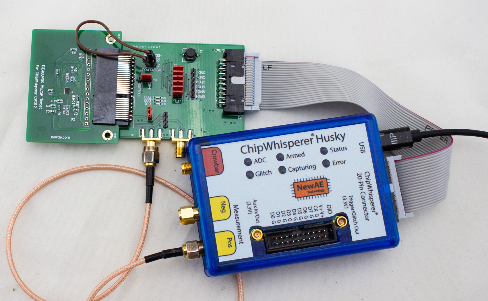
The soft-core in question is the excellent NEORV32 RISC-V core. I find that core’s got great documentation. You don’t need to build the core to use the existing design, as the ChipWhisperer repo has a pre-built binary of the FPGA image. So you can compile software for that image. But it’s fun to build your own core!
- Checkout the neorv32-setups repository.
- Follow instructions to configure the required FPGA toolchain (the ‘osflow’ toolchain).
- Run
make BOARD=iCE40CW312 MinimalBoot
Hardware ECC Attacks
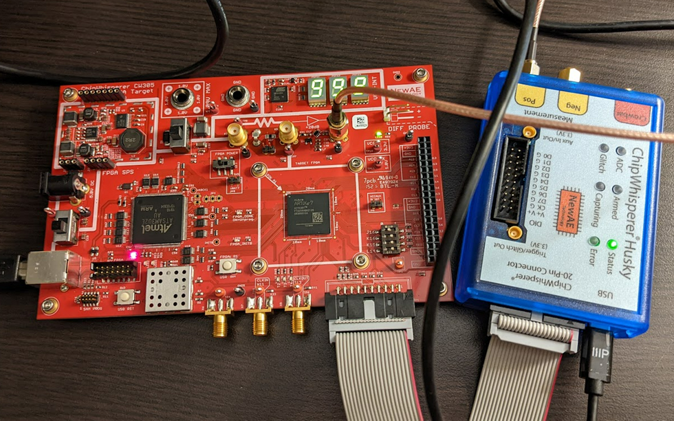
This demo uses the ChipWhisperer CW305 board (here in the A35 variant), which has a series of nice ECC jupyter notebook tutorials . These tutorials will walk you through how the entire attack works:
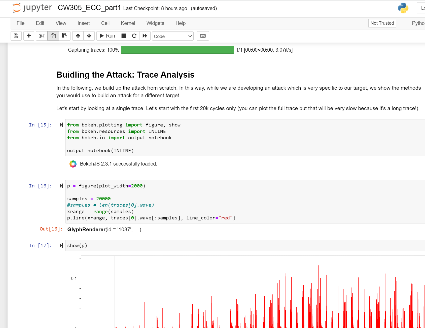
The ECC core is based on the excellent and open-source CrypTech project.
We have a detailed write-up of the attack that can also be helpful to see!
Apple AirTag Teardown & Test Point Mapping
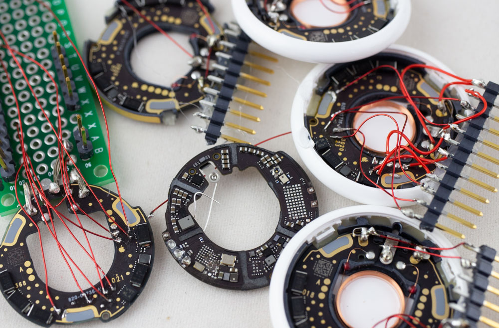
What’s inside of Apple’s new AirTag? There was already an iFixIt teardown (which I swear was missing a few items that are there now), but of course was curious to see what sort of protection was enabled. Notably the nRF chip used is likely vulnerable to a known bypass of security as well. With that in mind, I set out to see how we could dump some data from this thing – the good news is you can access a lot of interesting stuff (including the SPI flash) right from the backside, which requires you to simply pop the first plastic cover off. This is super-easy to do without damaging anything. Going further than that is tricky to keep it all intact.
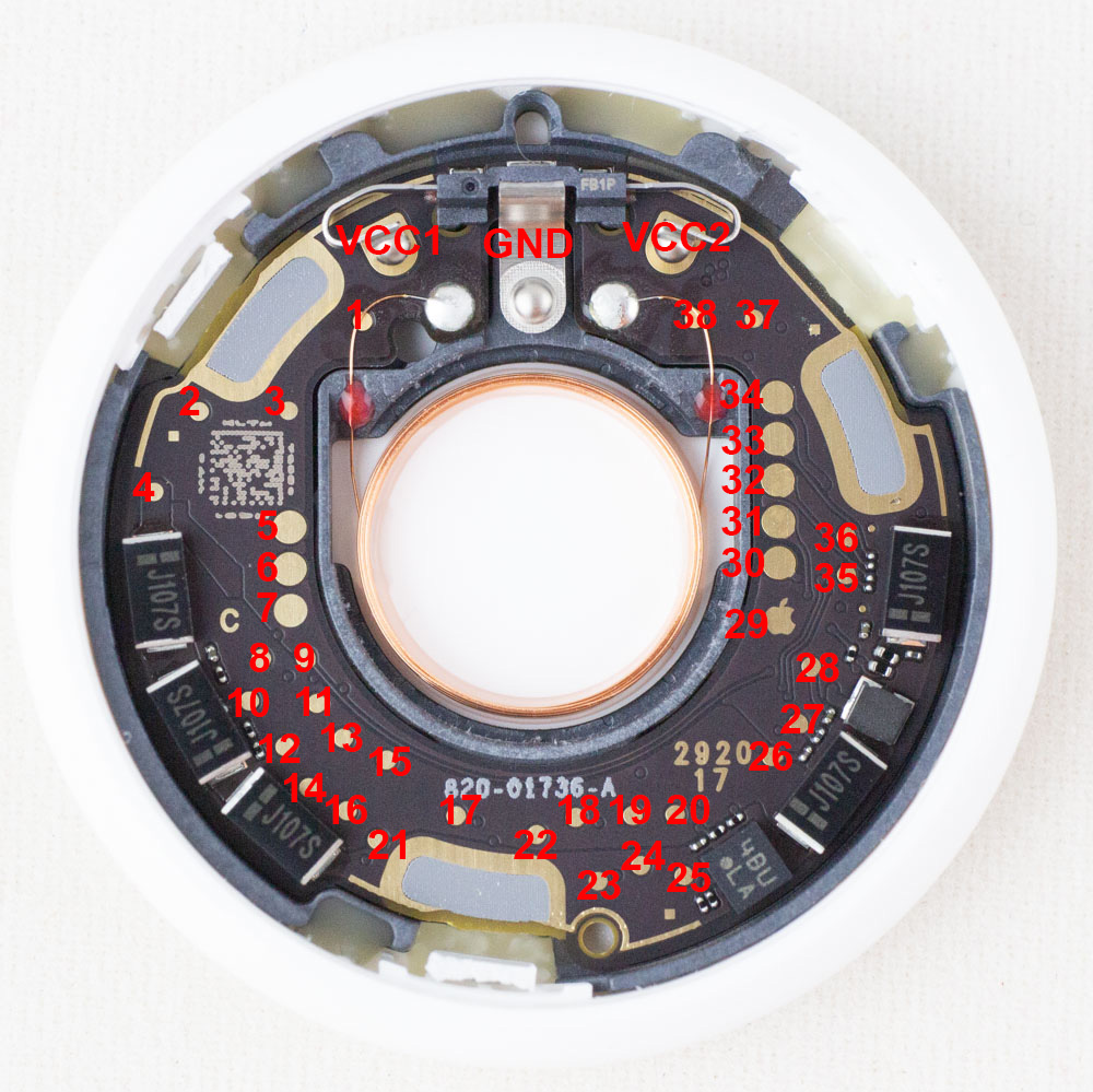
If you want to jump right to the answers, check out my AirTag-RE repo on github where I list the known test points that will be of interest. You can also see my twitter thread where I started the teardown:
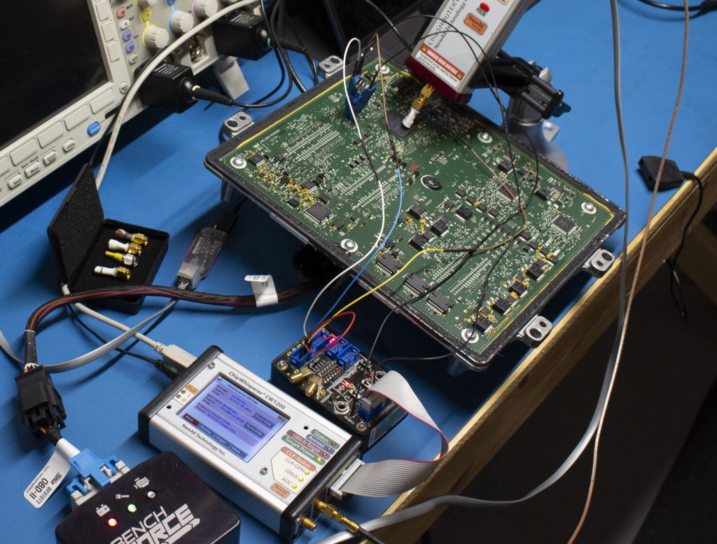
BAM BAM!! On Reliability of EMFI for in-situ Automotive ECU Attacks
This post is a summary of some work on an accepted paper for ESCAR EU 2020. This work was demonstration on certain NXP chips & GM ECUs, but the idea of both the attack & understanding how portable results are is applicable across the entire domain.
NOTE TO CAR TUNERS: I won’t perform this for hire on your ECU, please don’t email me asking this. The cost for me to do this type of work under hire would also be many times the HPTuners fee, and without any of of the actual tuning interface (I’m only attacking the bootloader, I never ever built a reflash tool that would be needed, yet alone the mapping work etc).
You can find links to:
🔧 The full technical paper in PDF
🔧 The talk slides in PDF
🔧 YouTube “video log” during work: Part 1, Part 2, Part 3, Part 4
This work was presented as a way to help automotive system designers understand the “real” threat to their systems, something that is hard to do when tuners hide their methods for commercial reasons. While I don’t know if the method I’m presenting is used by the car tuners, I assume some variant of it has been before (I doubt I’m the “true” discoverer). As I mentioned in the paper, I’m also not the first to turn EMFI onto automotive devices in an academic setting (another nice paper ref’d is the Safety != Security work). One contribution of my work is it directly talks about practicality, something critical for threat modelling but often skipped due to how messy this is. You can build the attack into a “portable rig” as shown here in a final demonstration:
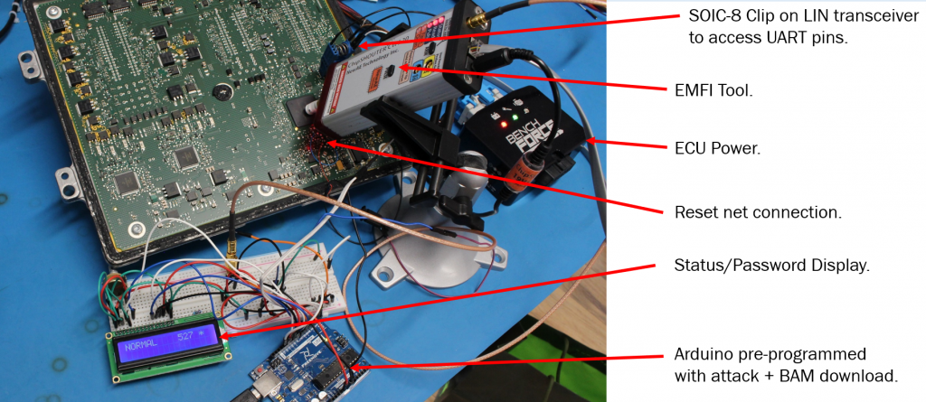
This portable rig is designed to show something along the lines of “pro garage” or “tuner garage” capabilities. It doesn’t need a ton of expertise to execute the attack, and opening up ECUs and probing them is widely done as part of regular tuning already (often called a type of “bench flash”). The real research wasn’t done with the Arduino setup, but instead using ChipWhisperer as part of the triggering with Python scripts searching:
The Arduino demonstration shown previously is not usable as-is for tuning. It’s very fiddly and hasn’t been optimized, so I can’t productize what was shown there easily (you can tell I get sick of people looking for tuning solutions…).
The attack is possible on these devices, as they have a hardware bootloader enabled with some pin on the board. This requires you to short that pin to GND to enter the bootloader mode, at which point the device is looking for a password. Using electromagnetic fault injection, you can bypass the password check such that an incorrect password is accepted.
You can use power analysis to discover some of the timing, as done in the paper. Comparing a good password to a bad password shows a clear point in time where the password logic differs:
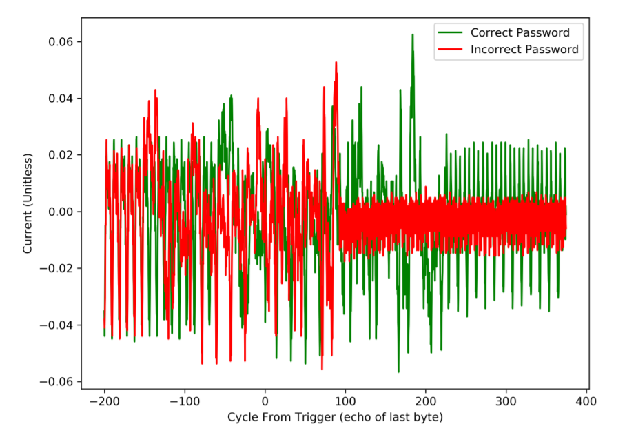
Interestingly, you can also see the red “incorrect password” trace appears to spin into an infinite loop (or similar), which would be around cycle 100 on the above figure.
As an important caveat: EMFI works against almost any microcontroller. Thus there is no “flaw” in the NXP MCU or GM usage of it, many other devices can be attacked using this same technique. The NXP MCU has long-term support (meaning it sticks around 15+ years), and was designed long before fault injection was on the radar of these devices as a realistic threat.
See the full paper for more details of the work.
Square Terminal Teardown
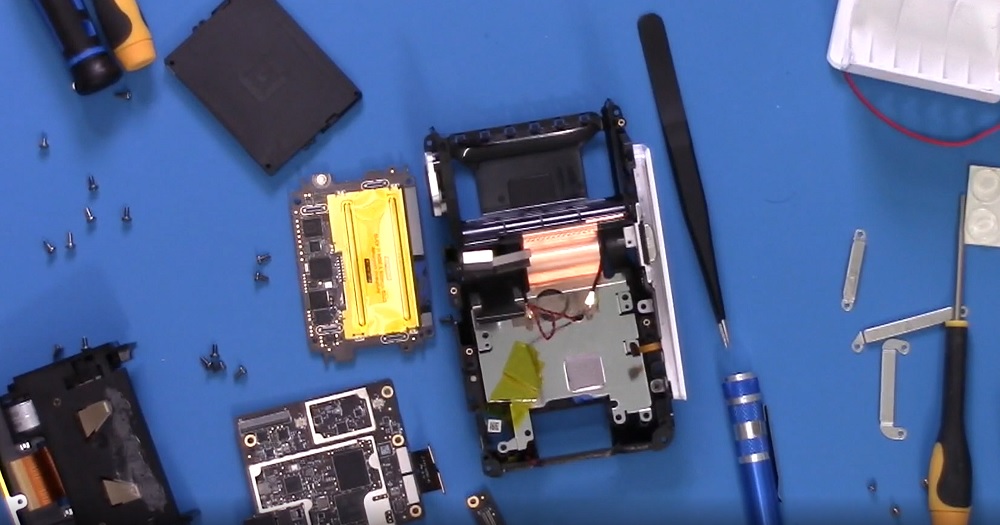
I recently tore down a square terminal (the one with the LCD screen) and wanted to share some of these results. I haven’t photographed everything as was mostly interested in how the secure areas of it are down. You can see an overview in the following video if you want to see how the whole thing fits together.
You can pull the main boards out to boot the thing on your bench (WARNING: as you see in the video above, this will trip the tamper circuits and destroy the device from being able to register/use):
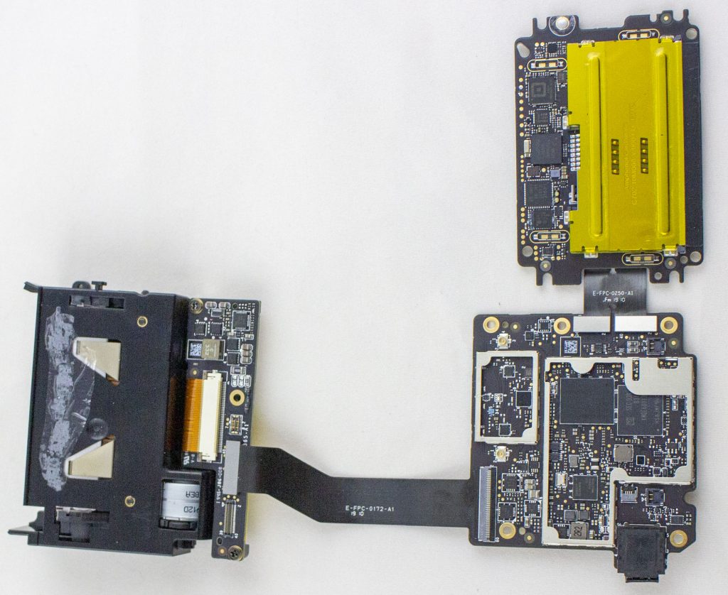
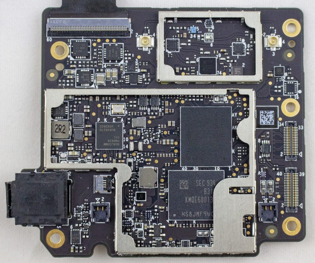
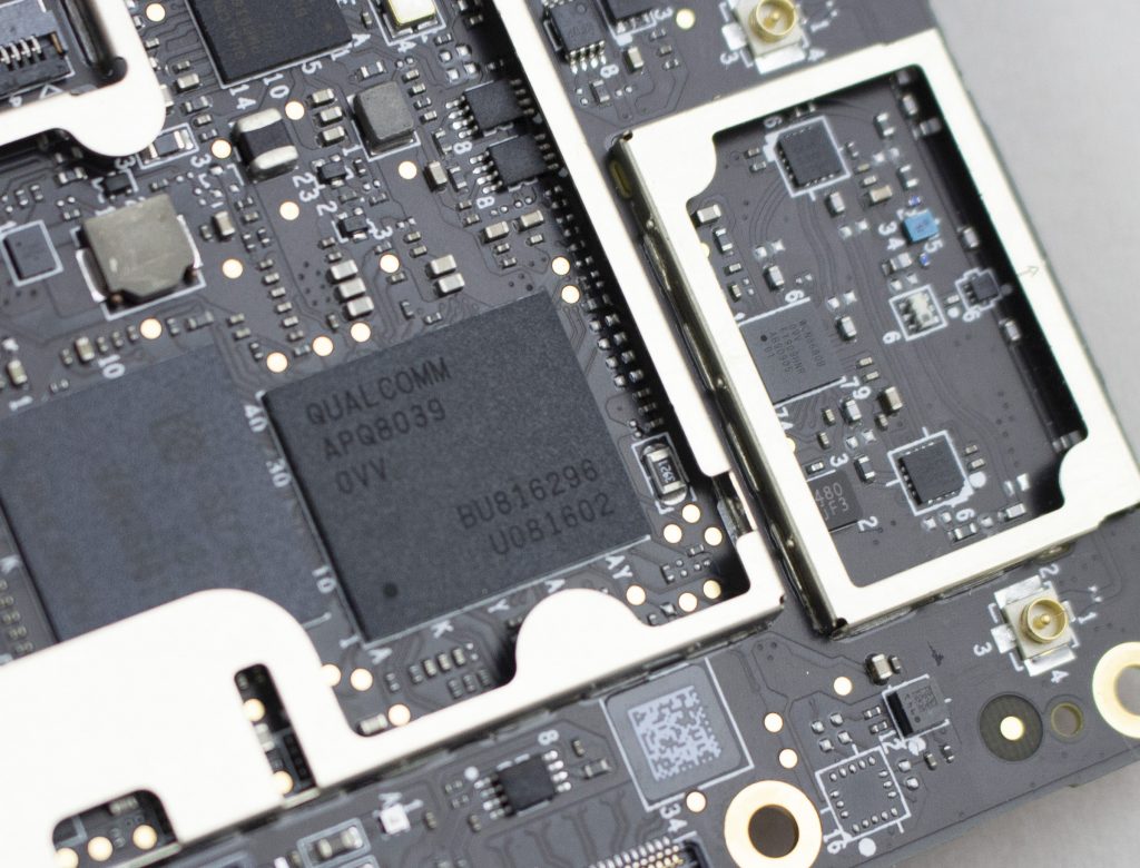
To start with the boring, here is the android board. It uses an APQ8039 (SnapDragon 615) as the main processor, with a KMQE60013M-B318 which integrates NAND (Emmc) and LPDDR in one package.
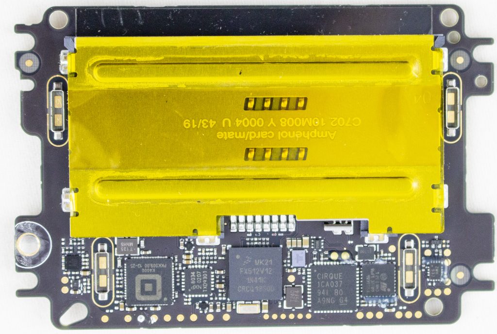
Alright, cool enough? While let’s get into the main stuff. There is a “security board” which I talk about in the following video:
This board features: MK21FX512 main microcontroller, a TDA9034 smartcard interface, a “Square K400Q”, a Cirque ICA037 touch controller, STM32F0, TS3A44159RGTR (analog mux), Lattice ICE5LP2K FPGA. Here’s a photo of the board with the taper screen removed:
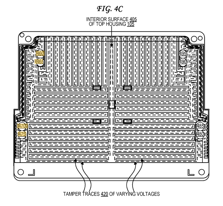
The tamper shield covers all of those test pads. Here’s a photo of the tamper screen:
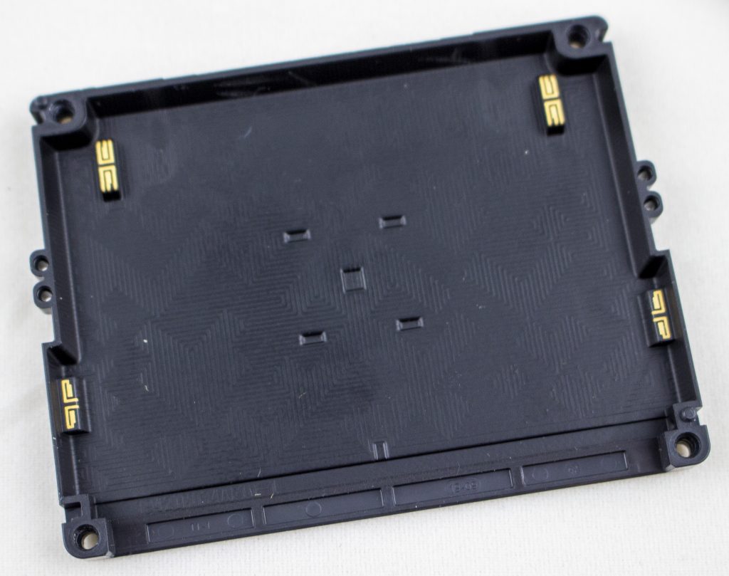
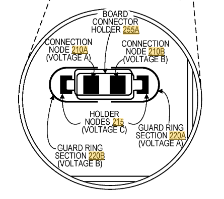
Very conveniently (for us), Square has filed a number of patents related to the tamper. In particular, here and here feature this exact cover:
I had measured out the connections, but the patent itself detailed them:
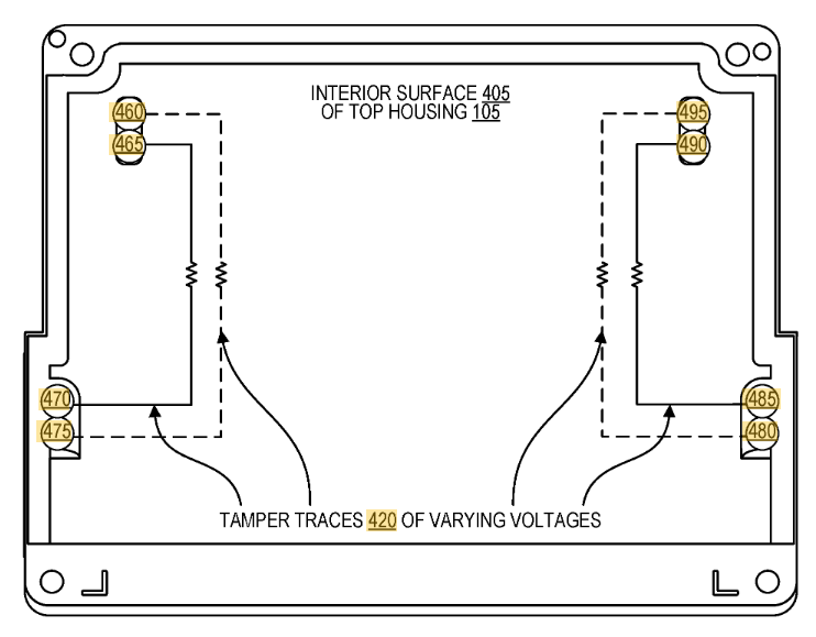
They patent also explains the land patterns on the PCB. The extra rings around it are for guard rings – if someone were to squirt some conductive glue into the enclosure, they would also trip the guard ring. Cool!
The other question of what is the Square K400Q device, which has a 13.56 MHz crystal hanging off it? While it turns out Square acquired a company called Kili Technology. And Kili Technology had a product called the K400Q, which is also in QFN-56 package. You can find the product page here (thanks to archive.org). No full datasheet, but it does have a short product brief:
What else is in it? Unclear exactly, but I would bet it’s using an enSilica RISC processor based on this press release. Unfortunately there aren’t public tools for it, although Lauterbach supports it in some form.
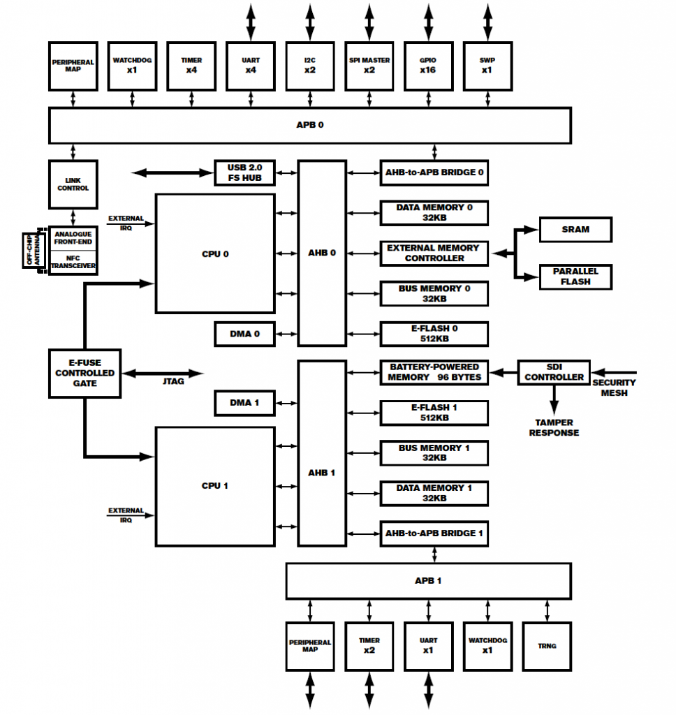
Finally – where is that security mesh handled? In my video I trace out some of it – the backup battery seems to run across the mesh on one side. The otherside seems to route to the STM32F0 processor. So it might be that the STM32F0 is performing some of the security mesh checking, which then triggers the Secure Destroy Interface (SDI) on the Square K400Q microcontroller. The STM32F0 has some epoxy blocking a few pins (very suspicious) as does the analog mux. The analog mux has some interesting-looking signals on it that make me suspect it is also part of the security mesh.
As a small side-note: all those test pads are right at the edge of the mesh. I haven’t tested yet, but I’m curious if you can dig down ‘under’ the shield without tripping anything. Or a very very fine shim may fit between the PCB & shield perhaps. Lots of stuff to test!
But that’s all for now. Project has been shelved for a bit, but hopefully you enjoy this look into the Square teardown!
MINOR UPDATE: I removed the epoxy around the STM32F0 – it looks like it might be near the mesh, but the mesh isn’t actually routing to the STM32F0 inputs (not 100% clear yet). The mesh seems to power the backup power for the MK21 instead, so it’s clear more effort is needed. Next step will be to remove the BGA on the MK21 so can probe where the mesh is going exactly.
Amazon Echo Dot Gen 3 – Microphone Disable Circuitry
Have you been interested in the Echo Dot device? One feature they mention is that there is a microphone off button. I spent a few hours reverse engineering this, and recorded (in un-edited glory) the process:
The resulting schematic is shown below:

The astute reader will note the only pin under direct control allows the disabling of the microphone, it cannot re-enable it. However – there is one more loophole to check.
The microphone comes up in an “online” state due to the strapping circuit. On quick check, it appears the 3.3V source is coming directly from a main 3.3V regulator which doesn’t seem to be controlled by the microcontroller. But I don’t guarantee there isn’t some way for the microcontroller to turn off the entire power, which if so would cause the microphone to be re-enabled when the device turns back on. It’s the last thing I’ll investigate, but will take some more effort to do so.
A Call for Time Travel Resistant Cryptography (TTRC)
At CHES 2019 [rump session], I presented my revolutionary talk on Time Travel Resistant Cryptography (TTRC). This is a hugely important area of research that has been widely ignored in academic work, and it’s time to finally make this right.

Why is this so critical? While Post Quantum Cryptography (PQC) gets NIST contests, and invested companies, nobody is considering TTRC. The general thought-process of PQC is that the existence of sufficiently powerful quantum computers is an open problem with no clear solution. BUT – if someone solves that problem (that is unclear is even physically possible to solve), it’s going to be hell on Earth for crypto implementations. Better safe than sorry.
That sounds a hell of a lot like some other problems to me.
And that problem even have had multiple movies made about it:

Lots of open questions exist. But note that many of them are not so unreasonable. For example – what if time travel requires us to create a Closed Timelike Curve (CTC), and time travel is only possible from the point that curve is created and onward.
This would mean that from the point the CTC is created crypto would immediately be broken, but any point before that (i.e., now) is safe. Thus we must create TTRC implementations since we cannot know when CTCs could be created.
I discuss many of these problems in my CHES 2019 Rump Presentation, you can see the slides below. When video is posted I’ll update this blog post with such material.
USB Triggering & Hacking
This blog post covers several topics that I should have made independent posts about… but anyway. Here we are. It’s September and I should have done this months ago.
Trezor / USB Hacking Updates (Black Hat + WOOT)
I had an earlier blog post with details of the Trezor attack. It turns out this is more generic type of attack than I realized, so I extended this work into a WOOT paper as well. Quickly I thought I should update on that…
To begin with – you can check out my Black Hat USA slides on the web at http://i.blackhat.com/USA-19/Wednesday/us-19-OFlynn-MINimum-Failure-Stealing-Bitcoins-With-EMFI.pdf .
Probably you want more details though, so luckily I included them in a paper presented at WOOT ’19 (see https://www.usenix.org/system/files/woot19-paper_oflynn_0.pdf).
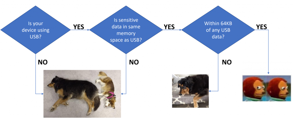
This paper includes some additional details. One major thing is that the USB attack I used in the Trezor applies to many other devices. Basically almost everything has something like the following chunk of code:
if (∗length > setup−>wLength) {
   ∗length = setup−>wLength;
}
The problem comes about because the wLength field ends up coming from the computer (host). Using fault injection we can always cause that code-path to be taken, meaning we can read out data directly from the target device. This applies in only certain circumstances… here is a quick flow-chart of when you should care:
PhyWhisperer-USB
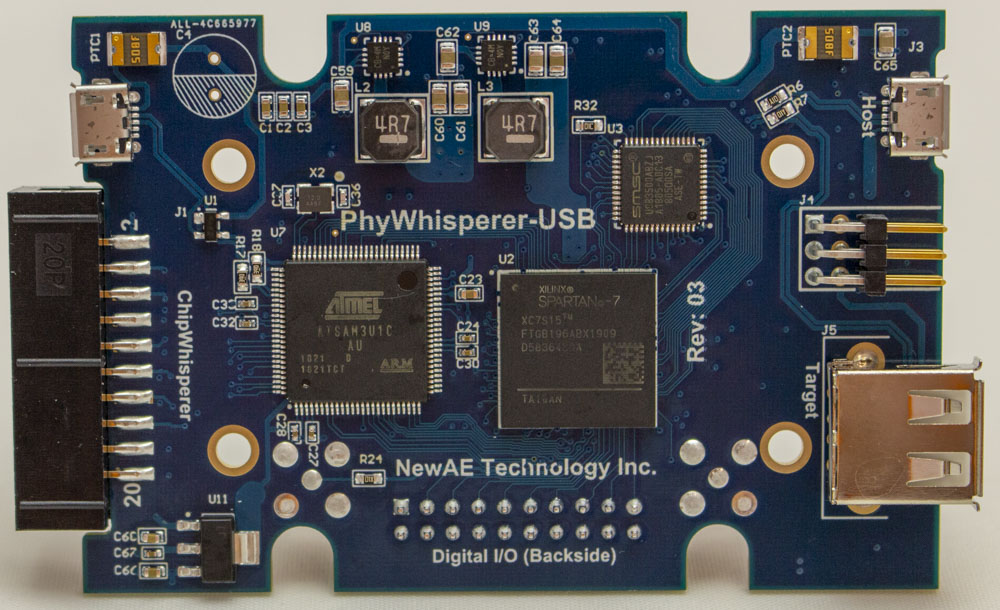
As part of this project, I also started a new open-source USB trigger logic device. You can check it out on
https://github.com/newaetech/phywhispererusb
We’re also doing a CrowdSupply for the initial run – see
https://crowdsupply.com/newae/phywhisperer-usb
FICHSA ChipWhisperer Tutorial Requirements
At the FICHSA Conference (
https://fichsa.sise.bgu.ac.il ) I will be running a short workshop on ChipWhisperer using the ChipWhisperer-Nano.
A direct link to a Google Doc with the most up to date information is available here: https://docs.google.com/document/d/1IgDeGZ6d0FEYJbaF4a-KsBhdIHlMZg04-wQYUSZgnks/edit?usp=sharing
If you want to fully play along, please bring a laptop with the following installed and setup:
- VirtualBox 5.x (5.2.28 is latest supported). You CANNOT use VirtualBox 6 due to some unknown incompatibility.
- VirtualBox Extension pack for version you installed (direct link to 5.2.28, does not depend on the host OS).
I will be (hopefully) posting a VirtualBox image once one is fully updated.
If you don’t need hardware and still want to see how the system works, please have a Google account – some of the work can be done on Google Colab.
See the Google Doc link above for more updated details (more detailed install / setup instructions etc)