NOTE: This article appeared in Issue 293 of Circuit Cellar, back in December 2014. I’ve posted it here for your reading pleasure as well. References to previous articles are for Circuit Cellar Issues, as this was originally written for the print publication. This version differs slightly from the print version – this is my own ‘author copy’ version before the Circuit Cellar editing. References to “ProgrammableLogicInPractice.com” are broken for now, but material has been mirrored to the bottom of this page.
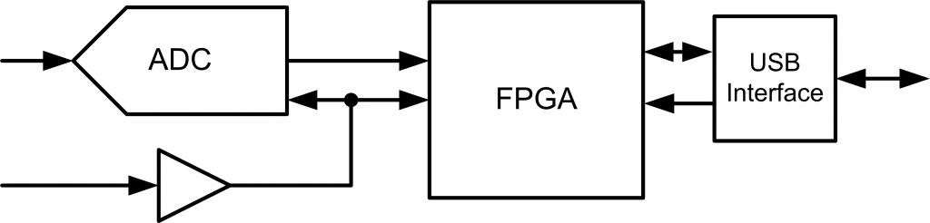
One of the most critical aspects of any FPGA design is where two clock domains meet. The general rule is to avoid this at all costs, but there are situations where it’s unavoidable. A simple situation is shown in Fig. 1, where our system is receiving data from an ADC, but speaking on a common bus. The ADC sample rate is generated from an external source, and might change for specific applications.
Figure 1: Systems such as this make it impossible to avoid multiple clock domains: the output of the ADC will be based on some external clock, and we also have some bus interface with a completely different clock. At some point data from the ADC clock domain must pass into the bus clock domain.Continue reading Experimenting with Metastability and Multiple Clocks on FPGAs
NOTE: This article appeared in Issue 315 of Circuit Cellar, back in October 2016. I’ve posted it here for your reading pleasure as well. References to previous articles are for Circuit Cellar Issues, as this was originally written for the print publication. This version differs slightly from the print version – this is my own ‘author copy’ version before the Circuit Cellar editing.
Back in December 2015, I discussed how I solder BGA devices
(such as FPGAs) using a low-cost reflow oven. This article will discuss the
design of the FPGA board itself, which you could then assemble using the tips
in my previous article.
I’ll assume you have a rough idea of what external parts you
need, as they will be highly dependant on what you are trying to accomplish
with your design. In addition to design-specific information, there are a few
standards external requirements such as programming interface, communications,
and power. This article will briefly cover some of these external requirements,
but the concentration of this article is how to physically lay-out the FPGA
board at a reasonable cost.
Some of the topics I covered previously too – for example in
my June 2015 article I discussed the use of a generic USB microcontroller as a
FPGA interface chip, which is very useful if you need to shuffle data to/from
the FPGA.
So let’s assume you have a (mostly) complete schematic, and
are wondering how to make this a reality. Let’s start with setting a target
goal in terms of board requirements.
PCB Specifications
Assuming this design will be either a prototype run or
possibly a small production run, it makes sense to design your PCB with
specific requirements in mind to keep costs reasonable. The two PCB
specifications you are most commonly told are the minimum “trace/space” (that
is, minimum width of a trace, and minimum spacing between copper features), and
the minimum drill size.
As I mentioned in my previous article, I’m often using an
overseas PCB fab at 3pcb.com, although many other options are worth trying. They
offer a variety of trace/space and drill size options, so I’ll target a 5 mil
space/trace with 0.2 mm drill. This is a fairly “standard” technology option,
so shouldn’t be a problem when moving towards a small production run (i.e., Qty
100-200).
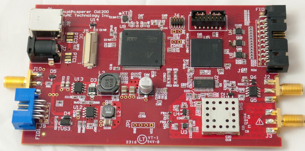
To give you an idea of what we’re working with, Figure 1 shows an example of the final PCB I designed and assembled. This uses a Spartan 6 LX45 FPGA with an Atmel SAM3U microcontroller for high-speed USB communications.
Figure 1: This 6-layer PCB features a Spartan 6 LX45 FPGA, an Atmel SAM3U microcontroller, and a 10-bit ADC. I’ll overview some of my experiences designing this board in this column.Continue reading FPGA Board Design Tips
I wrote for Circuit Cellar in a column titled “Programmable Logic in Practice” from 2013-2015. This column detailed various work around FPGAs. The column later became my “Embedded System Essentials” column, which primarily dealt with security issues in embedded systems.
The previous domain (programmablelogicinpractice.com) now redirects here. Unfortunately not all posts were transitioned. You can find copies of some of my articles if you check the Circuit Cellar tag.
I’ve got an article in the 25th-Anniversary edition of Circuit Cellar about the future of FPGAs. If you haven’t got an issue yourself yet, check out their webstore.
I’ve been working with Xilinx’s new High Level Synthesis tools built into Vivado. I’m slowly working on posting some more complete tutorials. In the mean-time here is a simple tutorial about making a Finite Impulse Response Filter on a real ADC/DAC board .