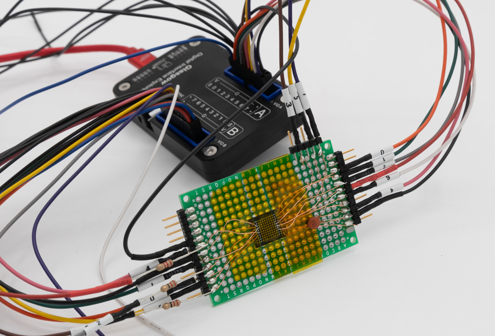
I recently got my Glasgow device, which is a rather impressive piece of tech. I followed the Windows installation instructions and it “Just Worked”, including installing the toolchain! On one computer I needed to use Zadig to force the driver to be libusbK, but on another Windows computer it wasn’t needed. In this blog post, I’m going to explore a parallel NAND device that I wanted to dump, and find out how well Glasgow works.
Continue reading Dumping Parallel NAND with GlasgowTag: tutorial
USB Inrush Testing
The USB spec has limits on the ‘inrush current’, which is designed to prevent you from having 2000uF of capacitance that must be suddenly charged when your board is plugged into the USB port.
The limit works out to around 10uF of capacitance . Your board might have much much more – so you’ll have to switch portions of your board on later with FETs as a soft-start.
For the ChipWhisperer-Lite, I naturally switch the FPGA + analog circuitry as to meet the 2.5 mA suspend current. Thus I only have to ensure the 3.3V supply for the SAM3U2C meets the inrush limits, which is a fairly easy task. This blog post describes how I did this testing.
The official USB Test Specs for inrush current testing describe the use of the Tektronix TCP202 which is $2000, and I don’t think I’d use again a lot. Thus I’m describing my cheaper/easier method.
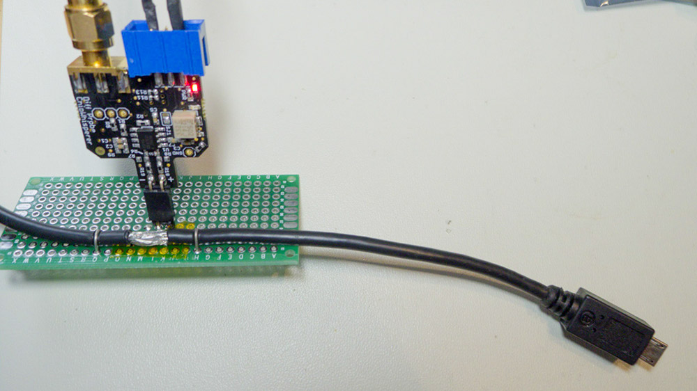
First, I used a differential probe (part of the ChipWhisperer project, so you can see schematics) to measure the current across a 0.22 ohm shunt resistor. The value was selected as I happened to have one around… you might want a smaller value (0.1 ohm say) even, as the voltage drop across this will reduce the voltage to your device. The differential probe has enough gain to give your scope a fairly clean signal. This shows my test board, where the differential probe is plugged into a simple 2-pin header:
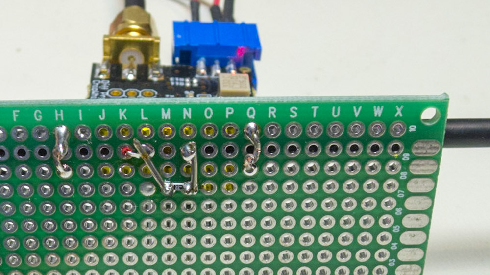
From the bottom, you can see where I cut the USB shield to bring the +5V line through the shunt:
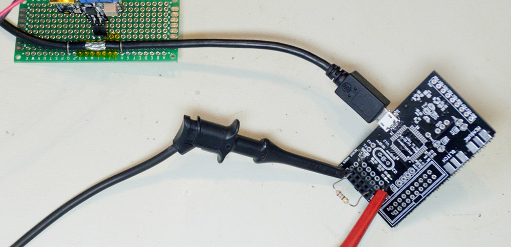
To calibrate the shunt + gain from the diff-probe, I just used some test loads, where I measure the current flowing through them with a DMM. You can then figure out the equation for converting the scope measurement to a current in amps.
Finally, we plug in our actual board. Here I’ve plugged in the ChipWhisperer-Lite prototype. The following figure shows the measurement after I’ve used a math channel in PicoScope to convert the voltage to a current measurement, and I’ve annotated where some of these spikes come from: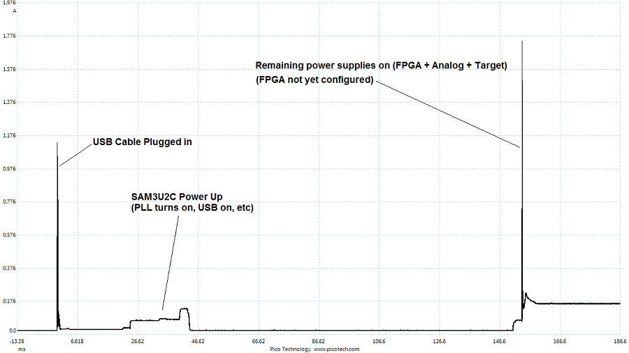
Saving the data, we can run through the USB Electrical Analysis Tool 2.0 to get a test result. The USB-IF tool assumes your scope saves the files with time in seconds and current in amps. The PicoScope .csv files have time in miliseconds, so you need to import the file into Excel, divide the column by 1000, and save the file again. Finally you should get something like this:
Note the inrush charge is > 50mC, but there is an automatic waiver for anything < 150 mC. While the system would be OK due to the waiver, I would prefer to avoid exceeding the 50 mC limit. In this case there’s an easy solution – I can delay the USB enumeration slightly from processor power-on, which limits the inrush to only the charging of the capacitors (which is done by ~15mS). This results in about 47 mC. This means I’ve got about 100 mC of headroom before I exceed the official limits!
This extra headroom is needed in case of differences due to my use of the shunt for example.
In addition, I should be adjusting the soft-start FET gate resistor to reduce the size of that huge soft-start spike. Ideally the capacitor charging shouldn’t draw more than the 500mA I claim when I enumerate, so that’s a little out of spec as-is! If I don’t want to change hardware I could consider using PWM on the FET gate even…
Design a FIR Filter in an FPGA in 30 mins using High Level Synthesis
I’ve been working with Xilinx’s new High Level Synthesis tools built into Vivado. I’m slowly working on posting some more complete tutorials. In the mean-time here is a simple tutorial about making a Finite Impulse Response Filter on a real ADC/DAC board .
Getting started with GIT Revision Control
Revision Control is the most critical part of any project involving files. Otherwise you end up with tons of directories, and naming schemes like “report_final2_june.docx” along with 20 other copies.
This is best described in this 20-min clip. Sorry it’s a little long, but there is a fair amount to cover:
You can download the slide set:
Slide Set
For your reading pleasure, here are the highlights. I’ve linked to the exact moments of interest in the video rather than retype stuff I describe in the video.
What is GIT
Git is a revision control manager. Briefly, it lets you see how things changed and track those changes. Even better, it lets you do tasks like create a “branch” of the source code. You can switch back and forth between branches to deal with issues like wanting to rewrite sections of the code, while still being able to get back to the last good ‘release’ copy.
Show Me Branching
Getting stated on Your Computer
You can use GIT on any folder! It’s dead simple to do, and handy even if you will never commit things to the web. Doing so requires a few steps:
- Create a repository locally Show Me
- Commit initial fileShow Me
- Commit changes Show Me
- Do other stuff (branching, merging, etc) Show Me
Using Real Repositories
To use real remote repositories, you need a server to host them. I recommend assembla.com or bitbucket.org . bitbucket.org provides more storage, more users for free, and unlimited project sizes for university-based projects. Both are pretty cheap for commercial projects.
You want to configure a SSH key. Doing so requires four steps:
Avnet Spartan-6 LX9 Board: Or How ChipScope is your Saviour
I was recently working on a project which needed more gates than I had in my trusty current FPGA Board (Spartan3-200 on DLP-FPGA-HS). I quickly found the Avnet Spartan 6 LX9 board (AES-S6MB-LX9-G), which I could buy for $90 and have here in a few days. It also comes with a license for SDK for ChipScope, as it’s designed for experimenting with on-FPGA processors. It doesn’t have a full EDK license so you are a little limited in peripherals…
But for my project I didn’t care about that. I was however interested in ChipScope Pro, having used it previously at a job. This quick post will show you how valuable it can be – the license included with the LX9 board is “device locked” and will only work with XA6SLX9 parts. ChipScope Pro is not normally licensed as part of WebPack so the $90 board is a great deal when you consider the licensing cost.
My normal FPGA debugging, beyond Verilog testbenching, is to use a LogicPort on some spare IO lines. This works well – the LogicPort has a very high sampling rate (200MHz external, 500MHz internal). But it requires a physical connection, which requires a lot of IO pins. I was hoping ChipScope could eliminate this problem.
There is two cores of interest: the Integrated Logic Analyser (ILA) core, and the Virtual IO (VIO) core. They are both controlled by the Integrated Controller (ICON) core. You can only have one ICON, but it can control up to a number of ILA/VIO cores.
The VIO core gives you a virtual dashboard, where you can toggle bits and see results. This is pretty handy for validating/playing with cores to check they function as intended. Here I am checking a UART core from fpga4fun.com:
Note the VIO core doesn’t provide buffering, so data is transferred over the JTAG. This limits your polling speed of course, but makes it easy to play with things. It does let you define pulse trains or single pulses if you have special timing requirements on e.g.: load lines, as I had here.
The ILA core is strictly input. But it connects to BRAMs on-board the device, meaning you can buffer a fair amount of data. Since it’s all on-device the speed is basically limited by similar constraints to the rest of your design. Of course if you already have a packed chip you might not be able to spare any BRAMs…
Here I am debugging a state machine, note you how can even define ‘tokens’ so it decodes the states correctly:
So the combination of ChipScope ILA + VIO I’m hoping will make designs go by a lot faster.
